


Microelectronic solder is an indispensable part of the assembly process of electronic products, which can effectively connect the various parts of the device together. With the arrival of the 5G era, electronic technology is developing in the direction of high power, high density and integration, and for the packaging of high-power devices such as IGBT, MOS, high-power LED, etc., it also puts forward higher and more comprehensive reliability requirements for welding materials. [1]
01 Status of several types of power device packaging
IGBT, a power semiconductor, is the core device of energy conversion and transmission, and the CPU of electric power equipment. The use of IGBT for power conversion can improve the efficiency and quality of electricity consumption, and has the characteristics of high efficiency and energy saving and green environmental protection [1]. Its application fields include industrial fields (such as frequency converter/inverter), household appliances (such as frequency conversion air conditioning, washing machine, etc.), and rail transit fields (such as high-speed cars, light rail, subway, etc.). In the field of new energy (such as new energy vehicles, wind power generation), medical field (such as medical regulated power supply), military aerospace field (such as aircraft, ships), it can be said that IGBT is everywhere in contemporary society.
In the entire IGBT module, one of the most important issues is heat dissipation, so there is an urgent need for good thermal management solutions, such as DBC ceramic copper clad plate, its materials involve alumina, silicon nitride, etc., there are more new materials in development, these materials are in order to better serve the thermal and electrical conductivity of the module, so the welding material is particularly critical.
IGBT assembly is divided into primary welding and secondary welding, primary welding is mainly welding chips, this part of the welding is mainly to establish the current path and heat dissipation path, the highest voidage requirements; Secondary welding is mainly for DBC baseplate, [2, 3] this part of the welding mainly plays a role in heat dissipation, IGBT module assembly structure is shown in Figure 1.
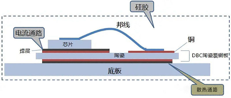
Figure 1 IGBT welding structure diagram
Welding IGBT module mainly uses solder paste and preformed tin sheet two forms of solder, welding requirements are as follows: industrial module, a single cavity rate < 1%, the overall cavity rate < 3%; In the field of new energy, the single cavity rate is < 1%, and the overall cavity rate is < 1.5%. For new energy vehicles, solder paste is difficult to meet such strict hollow requirements, and only some industrial modules will use solder paste. It can be seen that in order to better reduce voids and ensure stable low voids, IGBT module packaging is an urgent demand.
The welding process of IGBT is different from traditional reflow welding, which uses vacuum eutectic furnace + nitrogen + hydrogen (reduction), and also uses vacuum reflow furnace + nitrogen + formic acid (reduction). [4] In general, the high clean solder sheet can meet the higher void requirements, but when solder paste is used to weld the modules in the field of new energy, the void rate is difficult to stabilize below 1.5%. In addition, one of the problems often encountered by the client is the uneven thickness of the welding layer, which may be caused by the time of wetting and spreading when the solder is melted. [1, 4, 5]
The power device MOS for automotive electronics applications has a cooling pad at the bottom, and the size of the welding hole directly affects its heat dissipation, directly leads to heating and stress generation; For high-power LED, if it cannot guarantee its good heat dissipation channel, it will directly lead to the dead lamp of LED lamp beads, light decay and other problems. Therefore, the core of the so-called solution to heat dissipation is to greatly reduce the welding cavity [6].
02 Solder paste welding mechanism
The main components of the solder paste are thixotropic agents, rosin or synthetic resins, activators and solvents. The role of rosin: solid, chemical stability; When liquid, it can wet the corroded metal surface, and has a low enough viscosity to facilitate the removal of products; After welding, a stable insulation layer can be formed. The active agent mainly refers to organic acids, which are not decomposed before forming solder joints, otherwise the oxides cannot be removed. During welding, organic acids and water are formed by reacting with the oxides on the surface of the metal to be welded. Thixotropic agent and solvent determine the slump and viscosity of solder paste. Many organic acids are insoluble in rosin. Solvents are used to mix organic acids with rosin and spread them evenly on the surface of the solder joint to remove oxides. [7] In actual welding, about 10% of the solvent volatilizes below 130℃, and about 50% of the solvent volatilizes at 130-190℃. When the temperature reaches the melting point of the solder, the solder ball melts, the activator decomposes, and then cools, the flux forms a film, and the residue is fixed.
03 Causes of voids
The activator reacts chemically with the surface oxide of the metal to be welded, and there are mainly two types of reactions:
In the first reaction, soluble salts are generated, such as formula (1.1)~(1.2).
MeOn+2nRCOOH→ Me(RCOO)n+H2O …………….. 1.1
MeOn+2nHX → MeXn+nH2O…………………………… 1.2
The second is the REDOX reaction, such as equation (1.3)~(1.4).
MeO+2HCOOH → Me(COOH)2+H2O…………………. 1.3
Me(COOH)2+Me+CO2+H2………………………. 1.4
Both of these chemical reactions generate water, and some water may be absorbed during the use of the solder paste, and the volatilization of the solder paste solvent will also take away some water. During the welding process, if these water gases cannot be smoothly discharged, they will be directly retained in a hollow situation.
Secondly, in terms of substrate, PCB board moisture absorption, improper design of pad through holes, and different chemical treatment methods on the pad surface will lead to the formation of voids. The general void rate is OSP> in order; ENIG> Ag> Sn=HASL. [3]
The influence of the abrupt change of atmospheric pressure on the void should not be ignored. It is assumed that the atmospheric pressure is P0 and the air pressure of the return furnace is P1. When the air pressure in the furnace is negative, it is conducive to the discharge of volatile gases gathered in the furnace. Otherwise, the volatile gases in the furnace are not smooth or even blocked and remain in the solder ball to form a cavity. The influence of the temperature curve of the welding process can not be ignored, such as the increase of the constant temperature time, the hole is reduced, because the extension of the constant temperature time is conducive to the expulsion of solvents, water and other gases.
In addition, the higher the peak temperature, the cavity increases, because too high a temperature may lead to excessive expansion of the gas, the splash of solder, and the overflow of the gas in the PCB board.
04 A solution to hollowness
The causes of the above voids can be solved from three aspects:
1、Alloy improvement, adding trace elements to enhance solder wetting and spreading [6, 8];
2、Improved solder paste, the core of which is to add cavity inhibitor;
3、Continuous improvement of welding process.
For the improvement of traditional lead-free alloy, by adding trace elements Mn, Ni, etc., the preparation of new solder alloys, mainly improve the alloy properties of solder (usable), improve the process performance of solder (easy to use), improve the reliability of solder (stable and reliable). The purpose of increasing the trace amount of alloy is as follows:
1、Improve the wettability, fluidity, reduce the solder bridge and other bad welding and inhibit the crack;
2、Interfacial stabilization elements inhibit copper corrosion and interfacial IMC layer thickening;
3、Refine the addition of organizational elements, promote heterogeneous nucleation, and make the surface of the solder joint bright;
4、It retains the good ductility of traditional lead-free alloy, alleviating the expansion effect caused by the difference between the expansion rate of components and the PCB substrate;
5、The addition of anti-oxidation reduces tin slag, improves product stability and solder joint/coating durability. In addition, other options for alloy improvement are suggested as follows:
1) Add a certain amount of trace elements such as In, Ga, P, Ni, Sb to the alloy system to increase the fluidity and oxidation resistance of the alloy;
2) Oxygen content control of alloy powder;
3) Avoid using fine powder as much as possible;
4) Adopt preformed welding sheet technology.
In the experiment, the composition of the solder paste was optimized, and in order to improve the cavity, the researchers put forward a way to add a cavity regulator. That is, add an acid anhydride substance, and the reaction mechanism is as follows: It reacts with water to produce multiple organic acids, which continue to participate in the reaction and remove the oxides on the surface of the solder and the metal to be welded, thus reducing the influence of water on the cavity. The welding effect is shown in Figure 3 (X-RAY picture of IGBT welding after adding cavity regulator). Figure 2 is a comparison of Figure 3 (X-RAY picture of traditional lead-free solder paste welding IGBT), Figure 4 is the X-RAY picture of IGBT under the vacuum welding process of high clean solder. Figure 6 is the welding X-RAY image of IGBT after adding cavity regulator and trace alloying elements at the same time, and Figure 5 is the comparison picture of Figure 6. Figure 8 is the X-RAY image of MOS welding after adding cavity regulator in solder paste, and Figure 7 is the comparison image of Figure 8.
Secondly, the organic solvent as far as possible to choose a high boiling point solvent, to prevent the formation of splashing and other phenomena during the welding process.
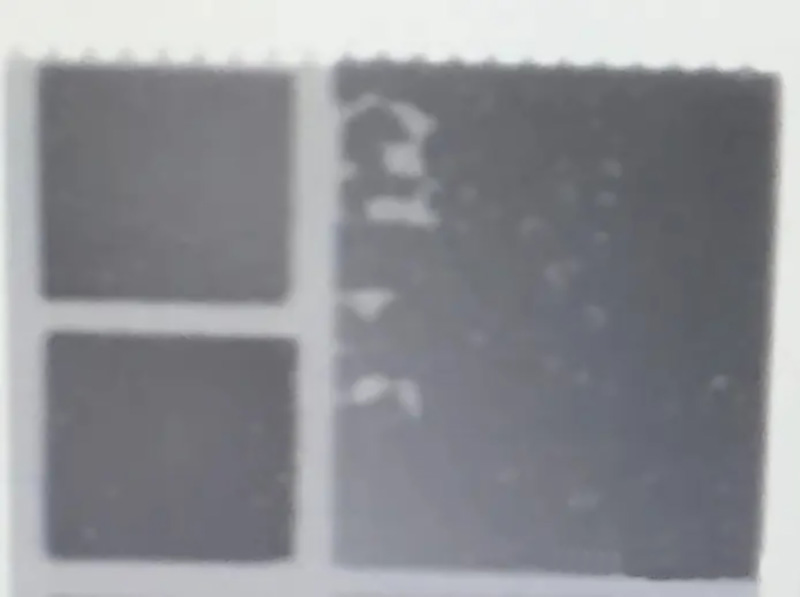
Figure 2 X-RAY picture of traditional lead-free solder paste welding IGBT
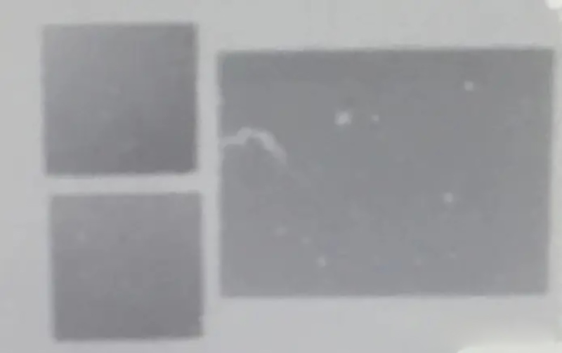
Figure 3 X-RAY picture of IGBT welding after adding cavity regulator to traditional solder paste
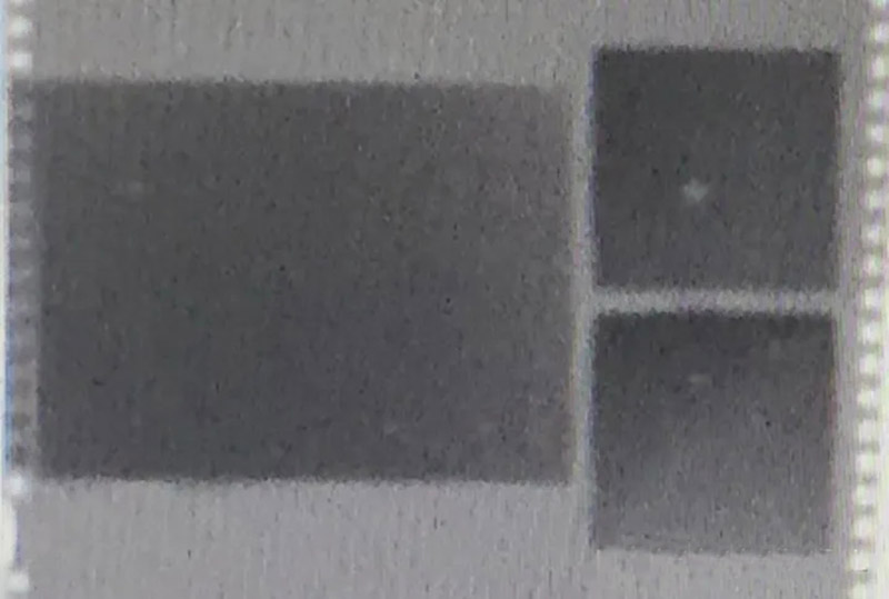
FIG. 4 X-RAY picture of IGBT in vacuum welding process of high clean weld
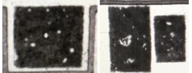
Figure 5. Welding X-RAY image of traditional lead-free solder IGBT
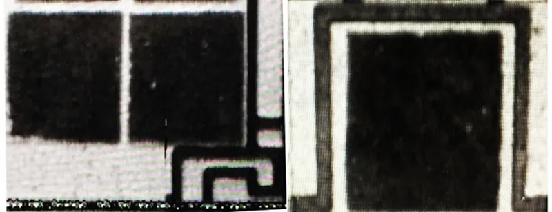
Figure 6. Welding X-RAY image of IGBT after adding cavity regulator and trace alloying elements
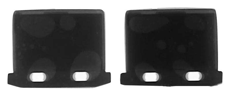
Figure 7 X-RAY image of conventional solder paste welding MOS
Figure 8 X-RAY image of MOS welding after adding cavity regulator in solder paste
Finally, the welding process should be continuously optimized as follows:
1) PCB moisture-proof treatment;
2) Control of the solder paste during use, it is recommended that the use time should not exceed 6 hours at room temperature to prevent the solder paste from being damp;
3) The reasonable setting of reflux curve, especially the setting of constant temperature time and peak temperature;
4) Control of ambient temperature and humidity;
5) Steel mesh opening methods, such as field, pit, oblique, etc., or a combination of several opening methods. 05 Conclusion
The fluidity and oxidation resistance of the alloy are increased by adding alloying elements. Adding the cavity regulator, acid anhydride, to react with the water generated in the welding process can effectively reduce the welding cavity caused by water vapor. Through continuous improvement of welding process, welding holes can be effectively reduced.