


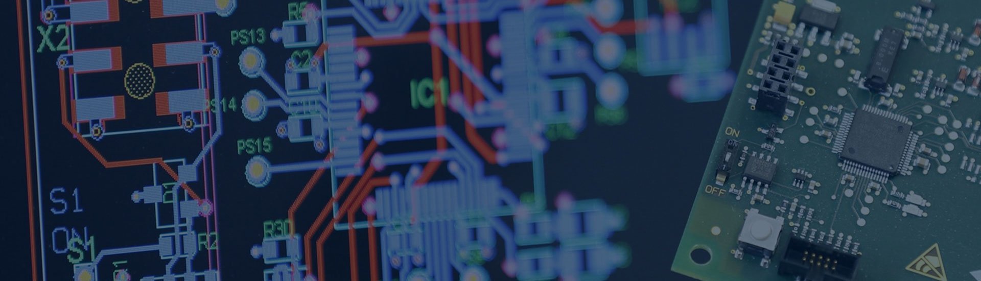
PCB Design and Layout Services
As a comprehensive service provider integrating PCB design and assembly, TORTAI provides full-process printed circuit board design and layout services, including:
- Component layout optimisation design
- Electrical signal path planning
- Customised development of circuit board structure
- High-density wiring solutions

We have an experienced and professional design team that can undertake all kinds of design requirements from basic single board to complex multilayer boards. Through continuous technological innovation and industry experience accumulation, we have successfully provided high-quality PCB design services for more than 100 industrial customers around the world.
Core areas of expertise:
- High-speed / high-frequency PCB design
- High reliability industrial grade circuit design
- Digital-analogue hybrid circuit design
- RF Microwave Circuit Design
- High Density Interconnect (HDI) design
Service Advantage:
- Design-manufacturing full-flow collaborative development
- Support 6-32 layers multilayer board design
- 100% compliance with IPC industry standards
- Provide DFM manufacturability analysis
- 24-hour rapid response mechanism
From PCB Design to Layout
- Min.trace width 2.5mil,
- Min trace spacing 2.5mil,
- Min vias 6mil ( 4mil laser drilling),
- Max layer count 32 layers,
- Min BGA spacing 0.4mm,
- Max BGA Pin 2500pin,
- Max High speed signal 12G differential signal,
- HDI highest Layer count 18 layers,
PCB Design & Layout Capabilities
| Min.trace width | 2.5mil | Min.trace spacing | 2.5mil |
| Min.Vias | 6mil(4mil laser drilling) | Max.layer | 48L |
| Min.BGA spacing | 0.35mm | Max.BGA Pin | 3600pin |
| Max.high-speed signal | 40 GBPS | Fastest delivery time | 6 Hours/ Item |
| HDI Highest layer | 22 L | HDI Highest laye | 14 Lany layer HDI |
Contact TORTAI Today For Best-in-class PCB Design And Layout Services!
