


Production and Inspection Capabilities
Tortai, not only provide PCBA one-stop service, but also provide customers with a variety of different materials, special processes, surface treatment of PCB circuit boards. Each piece of PCB adopts high quality raw materials and undergoes strict testing, each production link has QC special inspection, operator self-inspection, QA sampling product layers of control, factory products can be certified by UL, CE, MIN standards, ISO-9001, ISO 13485 :2016, ISO 14001 :2015, the EU SGS lead-free product certification. The company has experienced professional process team and quality control system, can provide a variety of special process PCB boards, such as: impedance board special ink (matte ink, purple, etc.) blind buried holes in the ultra-long, ultra-thin plate countersunk holes in the OSP process of thick copper boards, bare copper boards of high-frequency and high-speed HDI and so on. At the same time, we are also able to meet the needs of customers in various fields by providing a wide range of materials: FR4, Teflon, ceramic, halogen-free, high TG, mixed-pressure, ultra-thin and ultra-thick plates. Refined production process, providing a variety of surface treatment processes, such as: OSP, lead-free tin spraying, immersion gold, immersion tin, immersion silver, electro-gold, etc. Tortai promises that the quality of all products meets the industry’s standards before they leave the factory.
| Working Procedure |
Item |
Batch Manufacturing Capability | |
|
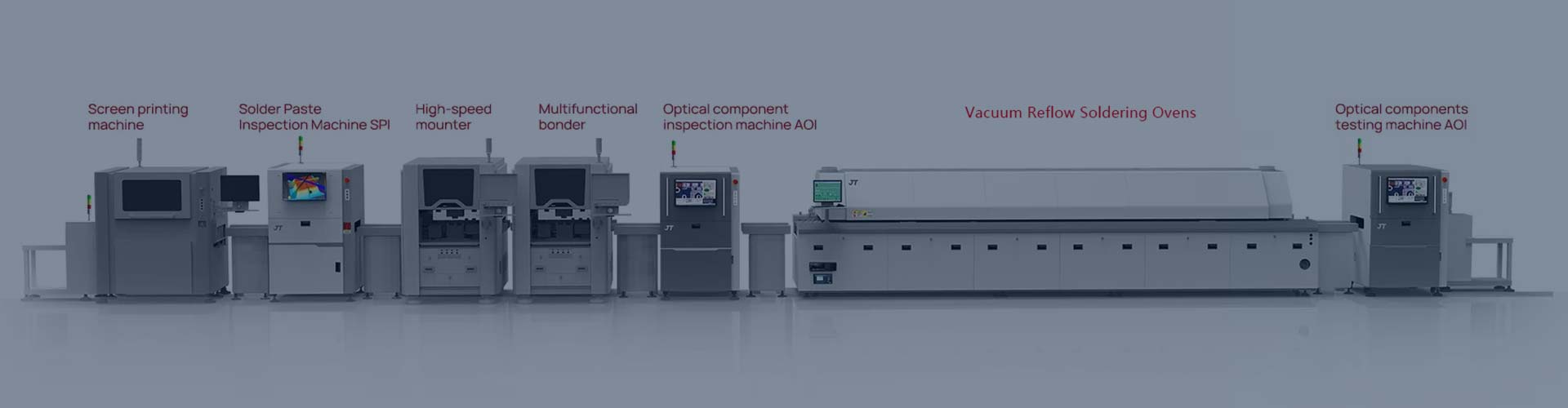
SMT |
Printing |
Maximum PCB Size Can Be Processed | 50*50 mm²—850*560mm², Proofing limit 1500MM length New Energy Control Board |
| Maximum Plate Quality | 8 kg | ||
| Actual Printing Accuracy | ±25μm(6σ) | ||
| System Calibration Repetition Accuracy | ±10μm(6σ) | ||
| Squeegee Pressure Detection | Pressure Closed Loop Control System | ||
|
SMD |
Processable Component Size range | 01005 , 0.3*0.15 mm² ,200*125 mm² | |
| Maximum Height of Processable Components | 25.4mm | ||
| Maximum Mass of Processable Components | 100 g | ||
| BGA/CSP Minimum Ball Pitch , Ball Diameter | 0.30mm,0.15mm | ||
| SMT Accuracy | ±22μm(3σ),±0.05°(3σ) | ||
| Range of Workpiece Sizes | Regular 50*50mm², Proofing Limit 850*560 mm² | ||
| Plate thickness range | 0.3mm–6mm | ||
| Maximum plate mass | 6 kg | ||
| Maximum Number of Material Types | 500 stations | ||
|
Vacuum Reflow Soldering |
Temperature Accuracy | ±1℃ | |
| Welding Protection | Nitrogen Protection (Residual Oxygen <3000ppm) | ||
| Minimum vacuum pressure | 0.1Kpa | ||
| Nitrogen control | Nitrogen Closed Loop Automatic Control System,±200ppm | ||
| Chip (IC) Bubble Void Rate Control | Vacuum reflow <2%, conventional air/nitrogen ovens (25%) | ||
|
SPI |
Detectable Minimum Pitch of Solder balls | 100μm | |
| X-Y Axis Accuracy | 0.5μm | ||
| Error Rate | ≤0.1% | ||
|
AOI |
Detecting The Smallest Components | 1005 | |
|
Detectable Bad Condition |
Wrong Material, Missing Parts, Reverse, Mounting Offset, Stelae, Side Standing, Open Welding, Tin, Turn Over |
||
| Bend Detection | 3D Inspection Function | ||
|
First Article Inspection |
FAI First Article Inspection System | High Precision LCR Bridge, Test Frequency: 50Hz-100kHz Basic Measurement Accuracy: 0.5%, |
|
|
3D X-Ray |
Magnifying Power | Geometric Magnification 2000; Systematic Magnification 12000 | |
| Rotation & Tilt Angle | Any ±45° + 360° Rotation | ||
| Resolution | 1μm /nm | ||
|
DIP/THT & Post- |
Preprocessing |
Automated Component Moulding Technology | Automatic Component Forming |
|
Plug-in |
Plug-in Technology | Automatic Insertion Machine | |
|
Wave Soldering |
Wave Soldering Types | General Wave Soldering, Selective Wave Soldering | |
| Inclination of Transport Rails | 4–7° | ||
| General Wave Soldering Temperature Accuracy | ±3℃ | ||
| Selective Wave Wave Soldering Stabilises Accuracy | ±0.06mm | ||
|
ACF Welding |
FPC (Flexible Printed Circuit) Connection to a PCB or Other FPC. | ||
| Chip-to-Substrate Soldering, Such as The Connection of IC Chips to FPCs in COF (Chip on Film) Packages. | |||
| Connection of The Touch Screen Sensor to The FPC or PCB. | |||
| Connection Between Sensor And FPC or PCB in Fingerprint Recognition Module. | |||
| Soldering of Other Electronic Components to Substrates That Require Fine-Pitch,High-Density Connections. | |||
|
Conformal Coating |
Maximum Processing Plate Size | 500*475*6mm³ ,Proofing Limit 1500MM Length New Energy Control Panel | |
| Maximum Mass of Veneer | 5 kg | ||
| Minimum Nozzle Diameter | 2mm | ||
| Other Characteristics | L700mm*W700mm | ||
|
Precision Gluing |
Itinerary of Work | Spray Pressure Programme Control | |
| Height Range | 0~100mm | ||
| Motion Tolerance | ±0.02mm | ||
| Proportion of Glue | 10:1-10:10 | ||
| Glue Viscosity Range | MAX≤20000 | ||
| AB Glue Output Tolerance | ±2% | ||
|
Box Building |
Assemble The PCBA, Power Supply, Connectors, Wire Harnesses, And Other Components Into a Complete Functional Box, Achieving Seamless Integration of Each Subsystem. | ||
| Conduct Functional Testing, System-Level Testing, And Environmental Testing to Ensure The Electrical Performance, Reliability, And Environmental Adaptability of The Entire System. | |||
| Optimize The Electrical Design of The Functional Box, Such as Power Management And Signal Integrity, to Improve System Stability And Efficiency. | |||
| Refine The Mechanical Design of The Functional Box, Selecting Appropriate Materials And Processes to Enhance The Product’s Structural Strength And Appearance Quality. | |||
|
Testing |
ICT Test |
Device Testing | Verify The Presence, Polarity, Value, and Functionality of Components. |
| Connectivity Testing | Check The Correctness of Connections on The PCB, Such as Short Circuits And Open Circuits. | ||
| Isolation Testing | Examine The Insulation Performance Between Wires And Between Wires And Ground. | ||
| Voltage Testing | Measure The Voltage at Specific Nodes in The Circuit to Ensure Compliance With Requirements. | ||
| Analog Circuit Testing | Assess The Performance Parameters of Analog Circuits, Such as Operational Amplifiers, ADCs, And DACs. | ||
| Boundary Scan Testin | Perform Functional Testing on Digital Circuits That Employ Boundary Scan Technology. | ||
|
FCT Test |
Functional Test | Verify That all Functions of The PCBA Meet The Specification Requirements, Such as Interface Communication, Key Input, Indicators, Buzzers, Etc. |
|
| Analog Test | Assess The Performance Parameters of Analog Circuits, Such as The Gain Bandwidth of Operational Amplifiers, linearity of ADCs/DACs, etc. | ||
| Environmental Test | Validate The Reliability and Adaptability of The PCBA Under Environmental Conditions like High/low Temperatures and Vibration. | ||
| Electrical Test | Examine The Electrical Performance of Power Supply, Memory,Flash Memory, etc., And Test The Stability of Voltage And Current. | ||
| EMC Test | Evaluate The Electromagnetic Compatibility of The PCBA to Ensure Compliance With Relevant Standards. | ||
|
Other Reliability Testing and Analysis |
Plating Analysis, Ultrasonic Inspection, Component Opening + Internal Visual Inspection, SEM Observation,EDS, Solderability Test,Temperature Cycling Test,acetone Corrosion, Electrical Performance Test, Chip Authenticity Analysis, Metallographic Section (Fixed or Non-Fixed Point), Plane Grinding, Cold And Hot Shock Test, Functional Test, Failure Analysis, Aging Test, ROHS Test, Drop, Vibration, Salt Spray, Water Immersion,Key Life And Other Tests. | ||
|
Programming |
Burning Mode |
Online Burning, Offline Burning, Fully Automatic Batch Burning | |
|
In-Chip Type |
MCU、FLASH、CUP、RAM、ROM、DDR | ||
|
Chip Brands |
Imported (ST, Tl, NXP, RENESaAS, MICROCHIP, etc.), Domestic (Zhaoyi, Xintang, Zhongying, Fudan Microelectronics, STC, Shanghai Beiling, etc.) | ||
|
Fixture Making |
Designing Customised Test Fixtures |
Product Load Test Fixture | |
| Simulated Product Usage Scenario Testing | |||
| Boot up Self-Test | |||
| Upper Computer Test | |||
| Tommunications Test | |||
|
Management Tools/ Software |
IMS |
The IMS System Covers Core Functions Such as Customer Management, Order Management,Procurement Management, Inventory Management, and Production Management,Significantly Enhancing Operational Efficiency and Information Transparency for Manufacturing Enterprises Through Real-Time Data Synchronization and Mobile Office Capabilities. The System Also Includes Financial Management, Data analysis, and Access Control Modules, Helping Companies Make Intelligent Arrangements in Cost Control and Operational Decision-Making, Optimizing The Overall Production Process. | |
|
MES |
Manufacturing Execution System, Mainly Used for Production Process Control, ECN Execution Control, Anti-Defective Control, Data Traceability, Etc. | ||
|
Component Explorer & BOM Manager System |
The System Provides Real-Time Access to Market Prices, Optimizes Inventory Management, Simplifies Inquiry and Quotation Processes, Facilitates BOM Allocation, and Offers Comprehensive Supplier Management. These Features Will Help Enterprises Improve Production Efficiency, Reduce Costs, and Optimize Supply Chain Management, Thereby Enhancing Market Competitiveness. | ||
|
DFM |
DFM Inspection Software Can Enhance Product Manufacturability, Reduce Production Costs, And Shorten Production Cycles. In PCB Design, DFM Encompasses Circuit Layout, Component Selection, Trace Width And Spacing, And Impedance Control Analysis. By Implementing Well-Designed DFM Practices, Product Manufacturability And Reliability Can be Significantly Improved. |
||
|
IP-Guard |
Intranet Security Monitoring System | ||
|
Corporate Certification |
Certification System |
ISO9001,ISO14001,ISO13485 | |
|
Quality Standard |
Manufacturing Standard |
IPC-A-630,Including Raw Material Procurement, Production Process, Process Control, Etc. | |
|
Test Standard |
IPC-TM-650,Including Functional Testing, Reliability Testing, Environmental Testing, Etc. | ||
|
Assembly Standards |
IPC-A-610 (level II); Includes Component Mounting, Soldering, Encapsulation, Etc. | ||