


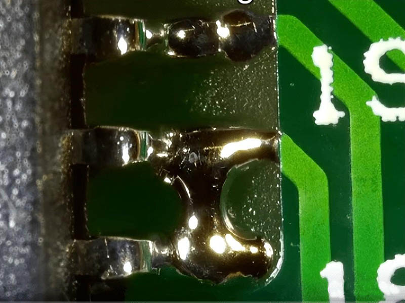
1、The solder bridge
Solder bridge is mainly solder across the two no electrical connection between the two conductors, which can lead to electrical short circuit. As shown below, the chip’s two pins are connected together.
Cause:
Solder paste printing process, PCB pad configuration of the arrangement of some differences with the actual.
Henkel deposition can also lead to, mainly the template aperture and pad ratio is too high.
Solder paste metal and flux ratio is not correct, resulting in solder collapse.
Too slow a heat-up rate in the preheat area.
Inaccurate placement can narrow the gap between pads, leading to solder bridges.
Solution:
The ratio of solder paste metal to flux should be well controlled.
Reflow temperature profile should be set properly
Ensure that the point pressure and accuracy of component placement
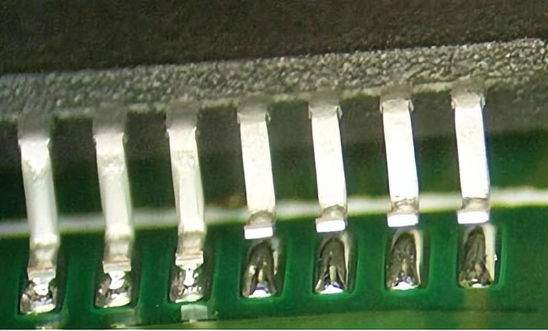
2、Insufficient solder joints / Void soldering
Void soldering and solder bridge is the opposite, there should be an electrical connection between the two points, not connected, it will cause an open circuit, as shown below.
Cause:
Insufficient solder, or solder paste clogging the holes in the stencil
Open circuits can also occur when there is enough solder, but the leads are not in contact with the pads during reflow.
Solution:
Correct the clump aspect ratio, which is defined as the ratio of the aperture width to the stencil thickness. Solder paste clogging the aperture may be due to an aspect ratio that is too small.
3、Solder Balls
Very small spherical solder particles are formed next to the joint. If there are too many solder balls, it is easy to cause false bridging and affect the function. If it is a water-soluble process, the impact is not significant and will be removed in the cleaning.

Cause:
Water saturation during reflow, resulting in solder balls
Too fast preheat does not provide enough time for solvent evaporation
Excessive oxides on the solder powder in the solder paste
Poor alignment of solder paste printing and solder paste factor on the soldermask and not on the pads.
Solution:
Use coarser powders, finer powders have more oxides.
Protect solder paste from moisture
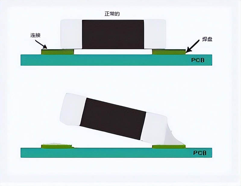
4、Standing monument
Standing monument as the name suggests is a chip standing up, one end is connected, one end is not connected.
Reason:
Before reflow, uneven prevention of components on the pad will lead to uneven welding force. Uneven heat distribution, solder melting speed is not the same, one side will be the first reflow, then it will lead to the chip standing up
Uneven heat sink, may suck the heat away from the pads
Solution:
The body of the component must cover 50% of both pads to avoid unbalanced soldering forces
Ensure that the temperature difference between the two ends of the component during reflow soldering is small
5、The solder is not tightly soldered together with the component
That is, the solder joints in the solder is not tightly soldered together with the components, will lead to the following figure:

Solution:
Use higher quality metal surface finish, such as higher temperature resistance OSP or ENIG.
6、Insufficient solder / Filler
The following chart, it is clear that the left side of the obvious solder is not enough, mainly the amount of solder paste than the template at the beginning of the design to be much less, after convergence, the solder is not enough to form rounded corners at the component pins.

Cause:
The aperture of the template is blocked by dry paste
The upper pressure of the squeegee should be appropriate, if the pressure is too high, it will lead to solder paste is brushed out, especially larger pads, it will lead to defects
Solution:
Split the large opening into smaller holes and check the squeegee pressure
Clean the stencil regularly
7、Cold solder joints
As follows, after welding, the surface of the solder joint presents a grey, porous appearance, normal should be bright and shiny.

Cause:
Insufficient heat absorbed by the solder
Before welding, the component is not clean enough, the solder impurities are more, this may also occur
Solution:
Adjust the reflow temperature, the solder can be completely reflowed
The above is about reflow soldering process is prone to 7 problems.