


Traditionally, the electrical connection between the IC chip and the outside is achieved by using metal leads to bond the I/O on the chip to the package carrier and through the package pins. As the feature size of the IC chip shrinks and the scale of integration expands, the pitch of the I/Os decreases and the number increases. When the I / O pitch is reduced to less than 70 um, the lead bonding technology is no longer applicable, it is necessary to seek a new technology path. Wafer-level packaging technology using film redistribution on the process, so that the I / O can be distributed on the entire surface of the IC chip is no longer confined to the peripheral area of the narrow IC chip, thus solving the problem of high-density, fine-pitch I / O chip electrical connection.
Among the many new packaging technologies, wafer-level packaging technology is the most innovative, the world’s attention, is a sign of revolutionary breakthroughs in packaging technology. Wafer-level packaging technology to wafer for the processing object, in the wafer at the same time on the many chips for packaging, aging, testing, and finally cut into a single device. It makes the package size reduced to the size of the IC chip, the production cost drops dramatically. The advantages of wafer-level packaging technology make it a great concern as soon as it appeared and quickly gained great development and wide application. In mobile phones and other portable products, has been widely used wafer-level packaging type EPROM, IPD (integrated passive device), analogue chips and other devices. The number of device categories using wafer-level packaging is increasing, and wafer-level packaging technology is a new technology that is developing rapidly.
In order to improve the applicability of wafer-level packaging and expand its scope of application, people are researching and developing a variety of new technologies while solving the problems that arise in the industrialisation process, to carry out research on the status, application and development of wafer-level packaging technology.
Wafer-Level Packaging
The initial germ of WLP was driven by the manufacture of low-speed I/O (low-I/O) and low-speed transistor components for mobile phones, such as passive on-chip sensors and power transfer ICs, etc. Currently, WLP is in the developmental stage, and demand is gradually growing, driven by applications such as Bluetooth, GPS (Global Positioning System) components, and sound cards. When it develops into the 3G mobile phone production stage, it is expected that a variety of new applications for mobile phone content will become another growth driver for WLP, including TV tuners, FM transmitters, and stack memory. As memory device manufacturers begin to gradually implement WLP, will lead the entire industry model change.
At present, wafer-level packaging technology has been widely used in flash memory, EEPROM, high-speed DRAM, SRAM, LCD drivers, RF devices, logic devices, power / battery management devices and analogue devices (regulators, temperature sensors, controllers, operational amplifiers, power amplifiers) and other fields. Wafer-level packaging is mainly used in film redistribution technology, bump formation of two basic technologies. The former is used to distribute along the perimeter of the chip soldering area is converted to the chip surface in the form of a planar array distribution of bump soldering area. The latter is used to create bumps on the bumped solder area to form a solder ball array.
Film Redistribution WL-CSP
Film redistribution WL-CSP is the most common process in use today. Because of its lower cost, it is well suited to the reliability standards required for high-volume, portable product board-level applications. As with other WLPs, the wafers for film redistribution WL-CSP are still made using the conventional wafer process. Before the wafers are sent to the WLP supplier, the wafers are tested in order to classify the circuits and map the wafers to qualified circuits. Before the wafer is redistributed, the layout of the device is evaluated to confirm that the wafer is suitable for solder ball redistribution.
A typical redistribution process results in a surface array layout of solder bumps, in which BCB is used as the redistributed dielectric layer, Cu is used as the redistributed connecting metal, sputtering is used to precipitate the bumps with a bottom metal layer (UBM), and screen-printing is used to precipitate the solder paste and reflow the solder paste, in which the bottom metal layer process is critical for reducing intermetallic chemistry reactions and improving interconnect reliability.
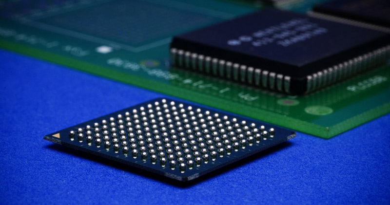
The redistribution process is to rearrange the I/O pads on the device surface. Figure 3 illustrates redistribution on bonded flash memory. As seen in the figure, the original pads on all four sides of the flash memory chip are converted to an array of bumps. In this example, two dielectric layers are used on the surface of the device, and a redistribution metallisation layer sandwiched between them is used to change the I/O distribution. After this process, the solder ball bumps are plated and the chip becomes a WLP product.
The disadvantage of designing the lead bond pads to be redistributed as solder ball array pads is that the WLP product produced is not likely to be optimal in terms of device design, structure or manufacturing cost. However, once it has been proven technically feasible, such circuits can be redesigned and the additional redistribution can be eliminated. There is a consensus that this is the case. A biphasic determination procedure has been specifically defined for this purpose. The next generation of changes may be the integration of a redistribution layer within the last metal layer of the chip, or a new design for the shortest signal line to improve performance.
The redesign may require the addition of new software tools. Redesigned signal, power, and ground lines are very inexpensive to construct because they eliminate the need for additional redistribution and related processes. Polymers are used for wafer flattening, to provide the necessary protection to the chip, and as a standard surface coating. The single-layer polymer WLP approach is a cost-effective design for thin film redistribution WLP.
Fabrication of Wafer-Level Microbumps
Leaded wire bonding has been considered a versatile and reliable interconnection technology since its inception 50 years ago. However, with the rapid development of mobile communications, Internet e-commerce wireless access systems and Bluetooth systems and Umbrella Ball Positioning System (GPS) technology, mobile phones have become the strongest and fastest growth driver of high-density memory, which is replacing PCs as the technology driver of high-density memory, with the demand for lower cost, smaller form factor, higher speed device performance, longer battery life, better heat dissipation, “green” process and higher device reliability has led designers to look to flip chip bump interconnect technology to replace traditional lead bonding.
The key technology driver for the development of PbTin bump technology is the continued tightening of device sizes. At 130 nm, approximately 30% of logic chips require bumping. However, at 90 nm, this figure jumps to 60%, and when it gets to 65 nm for mass production manufacturing, the need for gold bumping climbs to over 80%.
WLP based on BGA technology, is an improved and enhanced CSP. some people also called WLP wafer-level chip size packaging (WLP-CSP) which not only fully embodies the technical advantages of BGA, CSP, but also packaging technology to achieve revolutionary breakthroughs in the logo. Wafer-level packaging technology using mass production process manufacturing technology, can be packaged to reduce the size of the IC chip size, production costs have dropped dramatically, and the packaging and chip manufacturing into one, will completely change the chip manufacturing industry and chip packaging industry separation of the situation. Precisely because the wafer-level packaging technology has such an important significance, so it appeared on the emergence of great concern and quickly gained great development and wide application.
Under Bump Metallisation Layer (UBM)
In the flip chip interconnection method, the UBM layer is the key interface layer between the metal pads on the IC and the gold bumps or solder bumps. This layer is one of the key elements of flip chip packaging technology and provides a highly reliable electrical and mechanical connection between both the circuitry and solder bumps of the chip. The UBM layer between the bump and the I/O pads needs to bond well enough to the metal pads and wafer passivation layer; protect the metal pads during subsequent process steps; maintain low contact resistance between the metal pads and the bumps; can act as an effective diffusion barrier between the metal pads and the bumps; and can be used as a seed layer for the deposition of solder bumps or gold bumps.
UBM layers are typically achieved by depositing multiple layers of metal over the entire wafer surface. Techniques used to deposit UBM layers include evaporation, chemical plating, and sputter deposition. In advanced packaging, wafer bumping is critical from both a cost and technical standpoint. In wafer bump fabrication, metal deposition accounts for more than 50 per cent of the total cost. The most common metal deposition steps in wafer bump fabrication are the deposition of the under-bump metallisation layer (UBM) and the deposition of the bump itself, which is generally achieved by electroplating.
Electroplating technology can achieve very narrow bump pitches and maintain high yields. Moreover, the technology has a wide range of applications, allowing the production of bumps of different sizes, pitches and geometries. Electroplating technology has been increasingly adopted as the most practical solution for wafer bumping.
The UBM layer is firstly completed on the wafer. A thick adhesive is then deposited and exposed to form a template for the electroplated solder. After plating, the photoresist is removed and the exposed UBM layer is etched away. The final part of the process is reflowed to form the solder balls. The detailed process steps for making microbumps by electroplating are:
(1) Evaporation / sputtering of seed conductive layer (seed conductive layer) of the metal layer on the wafer;
(2) Rotationally coating a layer of photoresist on the wafer;
(3) Photolithography of the electrode window array pattern;
(4) Plating metal microembeddings through small holes in the photoresist;
(5) Removal of photoresist;
(6) Etching the exposed seed crystal conductive layer.
(7) Coating a thick layer of photoresist on the metal embedded body;
(8) Nesting out Au bumps;
(9) Etching away part of the thick adhesive so that the protrusion of the metal embedded body is revealed;
(10) Electroplating the Au bumps;
(11) Precipitation of a very thin Au or Cu layer on top of the embedded body.
Coplanarity refers to the consistency of the height of all bumps within a wafer, which has strict requirements in the flip chip bonding process. In flip chip bonding, variations in bump height can lead to uneven distribution of forces, chip fragmentation and electrical open circuits. Typical requirements for bump coplanarity are that the bumps should not have a height difference of more than 5 μm across the chip.
Thick film lithography
Wafer-level process technologies such as micro-pitch wafer bumps, lead pad redistribution and integrated passive components offer convenient solutions for many applications. Currently, many IC and MEMS devices have applied these technologies. With these technologies, device packaging and testing can be achieved at the wafer level before subsequent dicing processes. Typically advanced packaging techniques involve 5 to 100 μm thick film processes such as thick adhesive spin coating, uniform exposure of thick adhesive with large surface undulations, and obtaining very steep thick adhesive sidewalls. The iso-multiplier full-field exposure system is an equipment solution that can meet such needs with high throughput and low self-alignment costs, making it the most competitive system for projection steppers in thick-film lithography.
Wafer-level packaging processes include metallisation, lithography, dielectric deposition and thick film photoresist spin-coating, solder deposition and reflow soldering. The patterning process typically involves fabricating an under-bump metal layer (UBM) for the bump base with several layers of metal. The conductivity of the bump and wafer connection needs to be good, and the passivation layer and the underbump metal layer need to have good adhesion. The standard process flow for photoresist patterning consists of cleaning, coating, pre-bake, exposure, post-bake, development and firming. Each step of the process requires the definition of a set of parameters that have an impact on subsequent processes. After the photoresist has been patterned, the cavities are filled with solder or gold by electroplating or vapour deposition. The next step is to remove the photoresist and perform a reflow process in an oven to convert the cylindrical bumps into spherical bumps.
The thick photoresist coating will remain on the chip as a mask for fabricating micro moulds for metal solder joints. The redistribution coating can be retrofitted into a bump layout or used as a link between the peripheral pads and the area distribution pad arrays, which are made of 5 to 100 μm thick polysilicon films with different electrical, chemical, mechanical and thermal properties. Isolated redistributed area traces require materials with high strength, high thermal stability and low insulating factors. These materials have been successfully developed, one class of materials known as polyimide (such as DuPont developed PI series), another insulating material is the United States Dow Chemical Company (Dow chemicals) phenylpropylene cyclobutene (Cyclotene; BCB). PI and BCB are widely used in the flip chip bump package and other packaging processes.
Micro-featured dies for pads, bumps and under-ball metal layer structures using thick film photoresists can meet the different needs in WLP. Although the commonly used metallisation materials are SnPb, Au and Cu, several other materials can be applied for this purpose. Materials used for standardised applications require high resolution graphic conversion and easy stripping properties. Many practical applications require photoresist thicknesses in excess of 100 μm. in order to achieve such thicknesses, manufacturers develop suitable coating materials.
To meet these needs, manufacturers develop materials and process equipment. Many materials can be used to achieve “thin” photoresist coatings (i.e., 2-10 μm) on standard semiconductor process equipment. AZP4330 (Anchor Electronic Materials Group) and Shipleys 955 (Rohm & Haas/Shipley) photoresists are used to achieve photoresist layer thicknesses of 5 to 100 μm. Photoresist coatings of 25 μm film thickness can be achieved using a multilayer coating process, but this increases production time and cost. 25 μm thickness can be achieved in a single layer with AZ P4620 and SPR 220. For thicker coatings, the range of material and thickness options becomes smaller. When the desired photoresist coating is obtained with single-layer deposition, there are many benefits in terms of cost. Therefore, the development of photoresist materials with a thickness of 50 μm or more in a single layer is essential. For example, materials such as JSR THB-611P and AZPLP100XT from Anzhi Electronic Materials Group can achieve photoresist coatings with a thickness of 60 μm and above in a single layer. Recent research efforts have focused on achieving single-layer 65 μm thickness photoresist coatings using AZ9260 and single-layer 100 μm thickness photoresists using AZ50XT.
The thick film process has some special requirements for the system. The alignment system must be able to recognise the geometric pattern of the alignment marks uniformly over the entire adhesive thickness range and at specific heights of wafer surface undulation. This can be achieved using proximity lithography in combination with the shadow exposure principle, as the exposure source utilises parallel light exposure without relying on a focal point. The requirements of the lithography process for a proximity mask alignment exposer include high intensity, high uniformity, matching the wavelength of the UV light to the sensitive wavelength of the photoresist, sub-micron alignment accuracy, and maintaining an accurately controllable and consistent gap between the mask and the wafer during the exposure process.
EVG’s NanoAlign technology is designed to deliver the benefits of full-field exposure with the highest alignment accuracy and resolution and the lowest cost of ownership. The technology is now used in all of the company’s exposure machines. Targets include active anomaly control and sub-100 nm dynamic alignment resolution. Equipment includes specialised gluing equipment and contact/proximity exposure machines modified from standard models. The latest 200 mm EVG6200 Infinity and 300 mm EVG IQ Aligner exposure machines offer flexibility and a user-friendly interface for industrial production of φ200 mm and φ300 mm wafers that require a thick-glue process.
Wafer Thinning
Wafer thinning is critical in stacked chip packaging technology because it reduces the package mounting height and enables the stacking of chips without increasing the total height of the stacked chip system. Smart cards and RFID are an important part of the thinnest form of single-chip applications that reflect the requirements of thin wafers. Thinner chips can increase the reliability of thermal cycling and support thin products. But how thin the chip depends on the wafer diameter and the WLP process, the reason is: thin wafer surface is prone to produce damage, causing micro-cracks, as well as in the subsequent operation caused by wafer rupture. Since wafer backside grinding is the final step of the wafer processing process, the degree to which the wafer has to be thinned is limited by the WLP process. Therefore, viewing wafer-level packaging as an extension of the wafer process, the wafer process should be designed with the scope of applicability of the packaging process steps in mind.
Poorly matched coefficients of thermal expansion of silicon and mounting substrates are a significant cause of fatigue failure of encapsulated solder balls in thermal cycling tests and in field use. Also, this failure is closely related to how strong each component is on its own. The thinner the chip, the more flexible it is, and the more fatigue resistant the solder balls are bound to be. Therefore, thinning the wafer and thus reducing the chip thickness is also one of the most important measures to improve the reliability of solder bumps. Thinning the wafer before the wafer-level packaging process tends to deform or even break the wafer, which is not desirable. Wafer thinning after the completion of wafer-level packaging processing is a better approach, but the implementation is more difficult. Wafer-level packaging for the manufacture of wafer and thinning technology and equipment are under development.
Advantages of Wafer-Level Packaging
Wafer-level packaging based on BGA technology, is an improved and enhanced CSP, fully embodies the technical advantages of BGA, CSP. It has many unique advantages: ① high packaging processing efficiency, it is manufactured in the form of wafers mass production process; ② with the advantages of flip chip packaging, that is, light, thin, short, small; ③ wafer-level packaging production facilities, low cost, full use of wafer manufacturing equipment, no need to invest in a separate packaging production line; ④ wafer-level packaging chip design and packaging design can be considered uniformly, at the same time, which will This will improve the design efficiency and reduce the design cost; ⑤ Wafer-level packaging from chip manufacturing, packaging to the product sent to the user in the whole process, the intermediate links are greatly reduced, the cycle is shortened a lot, which will lead to a reduction in the cost; ⑥ Wafer-level packaging cost and the number of chips on each wafer is closely related to the number of chips on the wafer, the more the number of chips on the wafer, the lower the cost of the wafer-level packaging. Wafer-level packaging is the smallest size of low-cost packaging. Wafer-level packaging technology is the real sense of mass production chip packaging technology.
The advantage of WLP is that it is a chip-scale packaging (CSP) technology for smaller integrated circuits that significantly reduces die area while increasing yield due to parallel packaging and electronic test techniques at the wafer level. The cost per I/O can be significantly reduced due to the parallel operation of chip connections at the wafer level. In addition, the use of simplified wafer-level test procedures will further reduce costs. The use of wafer-level packaging can be achieved at the wafer level chip packaging and testing.
Wafer-level packaging technology trends
Wafer-level packaging technology should strive to reduce costs, continuously improve the level of reliability, and expand the application of large-scale IC. In terms of solder ball technology, Pb-free solder ball technology and high Pb solder ball technology will be developed. With the continuous expansion of IC wafer size and process technology advances, IC manufacturers will research and develop a new generation of wafer-level packaging technology, this generation of technology can meet the needs of φ300 mm wafer, but also to adapt to the recent emergence of copper wiring technology and low dielectric constant interlayer dielectric technology requirements. In addition, it is also required to improve the ability of wafer-level packaging to handle current and the ability to withstand temperature. WLBI (wafer-level testing and aging) technology is also an important topic to be studied. WLBI technology is to be directly in the IC wafer electrical testing and aging, which is important for wafer-level packaging to simplify the process and reduce the cost of production.
Conclusion: Wafer-level packaging technology is a low-cost mass production chip packaging technology. Wafer-level packaging is the same size as the chip, is the smallest miniature surface mount device. Due to a series of advantages of wafer-level packaging, wafer-level packaging technology is booming forward under the impetus of the demand for miniaturisation and low cost of modern electronic devices. Currently, wafer-level packaging technology is usually applied to small-sized chips with low I / O number. The industry also needs to develop new technologies to reduce production costs, the development of large-size chip wafer-level packaging and fine-pitch solder ball array wafer-level packaging.
Modern electronic devices to choose the type of package, both to meet the design requirements and the lowest cost. The existing level of wafer-level packaging is still only an optional type of packaging. To make the wafer level packaging technology to become the mainstream manufacturing technology for future large-scale products, there is still a lot of work to be done. Designing semiconductor chips in conjunction with WLP packages will undoubtedly benefit the layout of WLP devices and improve device performance. In WLP, batch processing reduces packaging costs because the packaging steps for all devices on a wafer are performed simultaneously.