


One of the most common physical repairs on a PCB (restoring the functionality of a defective PCB but not meeting the original specifications) is solder mask repair. The purpose of the solder mask is to prevent solder from flowing from one point to another during the initial assembly process. The damage to the solder resistance film (Figure 1) may be cosmetic or functional in nature, for example, a situation where the solder resistance film preventing the downward flow of solder from the BGA to the “dog bone” type causes the BGA ball solder joints to be “inadequate”, which in turn leads to defects.
Solder mask issues

Figure 1: Solder resistance film defects
There are several ways to damage the solder mask. Lack of solder resistance film may occur due to broken adhesion between solder resistance film and PCB. When using uncontrolled heat sources and solder braiding strips to remove solder from pad locations, the solder mask may also be damaged, such as scraping the solder mask off. If the solder mask is exposed to multiple thermal cycles, the solder mask may become brittle and crack (Figure 2). Poorly adhered solder mask may cause solder shorts, other welding abnormalities, or cause solder mask to flow down the dog bone from the BGA pad.

Figure 2: Example of solder resistance film adhesion problem
Several different techniques can be used to service solder resistance films, each with its own advantages and disadvantages. One method outlined in section 2.4.1 of IPC-7721 is the use of a liquid solder mask. It can spread to areas in need of repair. This alternative mask is then cured by heat or ultraviolet light. After reading the manufacturer’s instructions, selectively apply the UV-curable solder mask and place it under the correct wavelength UV lamp. Based on the output of the UV lamp (which can be measured using a radiometer), the curing time of the given solder resist film and the distance between the lamp and the solder resist film, the service technician can record the controlled process.
Another method (Figure 3) is a simple technique of “point” welding mask repair by using a repair “pen” (IPC 7721 2.4.1), usually cured by air drying or baking cycles. The liquid oozes from the soft nib, which can then be air-cured or heat-cured. The nib itself is large relative to the size of modern BGA pads, so accurately applying the solder film material is a challenge. Due to the porous nature of the dot coating head, it tends to collect debris (including flux residues, residual masks, and cleaners) from the board. This absorbed debris can then re-contaminate other areas of the board. Personnel who use this technology to repair solder mask require an advanced level of skill, and even then, often do not have the skills to repair the appearance of solder mask compared to the methods outlined in 2.4.1 in IPC-7721.

Figure 3: Repair solder resistance film spot using repair pen
In addition to this method of repairing the pen, there is another technique that uses a polyimide, adhesive-supported in-situ mesh board to repair the solder resistance film underneath the BGA. This is a reliable way to place BGA while servicing the solder resistance film. The advantage of this mesh is that the BGA can be simply placed while also providing isolation between pads to prevent short circuits between I/ OS. This method can fix the lifting height between the BGA base and the PCB to control the collapse height, and at the same time serve as the solder resistance film “auxiliary tape”. When installed in place, the mesh plate acts like a solder mask repair template. This allows even technicians who have just started repair work to repair the damaged solder mask underneath the BGA.
Finally, there is the solder resistance film repair screen technology (Figure 4). This method can save maintenance time when a large area of solder mask needs to be repaired. Ultra-thin mesh panels define the solder mask area required for service. The replacement solder mask material is scraped into the mesh holes and then cured. After curing, the mesh plate is stripped, leaving a hardened replacement solder mask in its path. Although this method can save time for multiple boards that need to be repaired in exactly the same area or very complex large area repairs, it requires a service technician with an advanced level of skill.
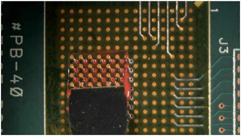
Figure 4: Mesh method for servicing multi-position solder resistance film
As with all PCB repairs, the customer must be notified in advance if the solder mask needs to be repaired while the PCB is being serviced. There are a variety of repair methods based on the purpose of assembly, cost and complexity of servicing the solder mask required.