


What is PCB Design? Summary of 18 PCB assembly design skills to help you avoid DFM problems
As an NPI engineer, DFM manufacturability analysis covers a wide range of areas, and today it is closely related to DFM, mainly about PCB assembly design techniques.
Today is mainly to share PCB assembly design (DFA), PCB assembly design tips.
- What is PCB Assembly Design (DFA)?
- PCB assembly combines a circuit board with other electronic components such as connectors, housings, heat sinks, etc. to embed them into the final product.
PCB assembly design: It is to consider PCB assembly during the early design phase to obtain the best product.
There is a frequent problem, which may be that those PCB design bosses will make fewer mistakes, but it is still a common mistake for novices, that is, the initial circuit board design is not fully considered assembly. Instead, more attention is paid to the PCB itself, without a broad understanding of the problems in the manufacturing process.
Ignoring PCB assembly can lead to a series of concurrent symptoms.
- Individually, the PCB design seems to be completely acceptable, but there will be huge problems in the later assembly, for example: the components may be too close to each other, and the subsequent products cannot work or the performance is problematic.
- The availability of components, if the components cannot be used, the entire manufacturing process will be delayed.
So how do the average PCB layout boss avoid making these mistakes? If you are considering PCB assembly design, here are 15 PCB assembly design tips.
Second, PCB assembly design skills
- Pay attention to the gap between components
One of the most common questions asked by PCB Layout bigwigs: component-to-component spacing.
Being too close to each other creates problems that may require redesign and remanufacturing, resulting in lost time and money.
PCB layout bosses typically design this way that there is enough gap between component boundaries to mitigate potential problems caused by components being too close.

Place components around silkscreens and assembly lines

Component spacing diagram
PCB Layout engineers must carefully position components to prevent overlapping shapes, and in the image above, you can see that 50 mli spacing is maintained between components.
In general, routing and layout rules are required, such as a minimum spacing of at least 10 mils between discrete components such as capacitors and resistors, where 30 mils is preferred. There are some other spacing rules, see the image below.
The above pitch values are for reference only and are subject to availability.
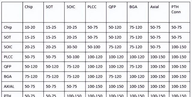
Component spacing value
- Select good components in the design stage
Experienced PCB Layout engineers select components early in the design process to ensure that there is no conflict between the design and the actual assembly.
By considering component size and space at the beginning, there will not be so many problems in the PCB assembly process.
Smaller components generally take up less space on the PCB, so you need to consider whether you can reduce the size of the component.
- Separate leaded components from lead-free components
It is important not to mix lead-free components with leaded components, and if any component requires lead-free assembly and no traditional leaded solder alternatives are available, the entire PCB must be lead-free and all components must be lead-free assembly.
Sometimes, the only package available for a particular device is Pb-free BGA. But generally speaking, there are some specific requirements.
The separation tabs left between the PCBs after routing interfere with the assembly of connectors extending to this edge, and the following problems arise when board manufacturing and assembly are not tightly coordinated.
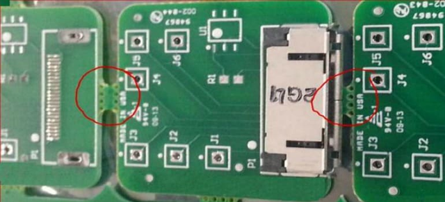
Separation tabs between PCBs
- Evenly place large components
Distribute large components as evenly as possible on the PCB board during layout to achieve optimal heat distribution during reflow soldering. Ensure that the PCB vendor develops a reflow curve for the reflow soldering volume.
- The chip components should not be too close to the edge of the PCB board
SMD elements are ideally 150 mils (3.8 mm) from the edge, especially if V-grooves are used.

- Do not use very small drills
Drilling like 6 mils is almost the smallest mechanical drilling and is not recommended unless there is no other choice. Due to BGA density, 18.5/8 (18.5mil pad/8mil drilling) is recommended, ideally 22/10 would be fine, but BGA does not allow it. (Data is for reference only, subject to availability)
15/6 mil via design
- SMD is at least 150 mils away from THT
This facilitates selective wave soldering or wave tray assembly.

The bottom chip element is too close to the TH hole
- Correct definition of mounting holes
Typically, a mounting hole is a tool hole defined in the drill drawing with an appropriate center point and drill diameter. Define it with a cut, but instead of placing the mounting on the drilling table, it is done in a less precise wiring phase.

The mounting holes are not defined correctly
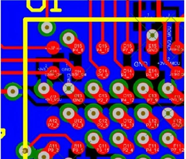
- The gap of the mounting hole
If there are other components, sufficient clearance must be maintained around the mounting holes.

Insufficient clearance to the mounting holes to the connector
- Avoid mixing manufacturing process
Avoid mixing manufacturing processes as much as possible. For example, if you use plug-ins, try to put all the plug-ins on the same side of the board, which can reduce the cost and time of PCB manufacturing and assembly.
- Select the appropriate package size
The components used in the design should be carefully examined at an early stage of the layout, and if there is enough space on the PCB board and the current design does not require the use of small package components, larger components are required, which makes more use of PCB assembly.
For example, use the resistor of 0402 instead of the resistor of 0201 whenever possible. If the resistor of 0805 can meet all the requirements, then the resistor of 1206 will not be selected, which can reduce the size of the PCB.

PCB size
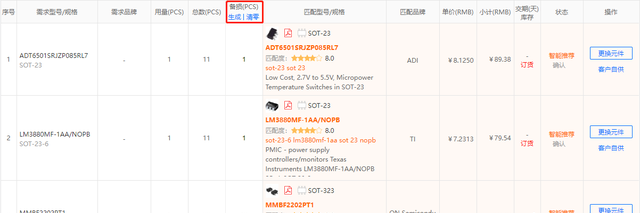
- Find components with suitable cycle
As mentioned earlier, the availability of components can cause serious delays, so it is necessary to check the inventory, delivery time, and discontinuation of components at the design stage. This can be found on various electronic component websites.
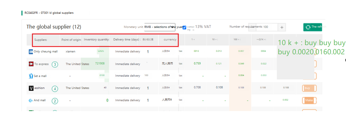
Component delivery time, inventory (from core mining network)
- Keep the BOM up-to-date when designing
The bill of materials (BOM) is a key aspect of design and assembly.
If you have any issues with your BOM, the PCB factory will pause the project until it is resolved with the engineer.
One way to ensure that the BOM is updated is to review the BOM at any time when the design changes.
When you add a new component to the schematic during layout, make sure you also update the BOM with the correct part number, description, and component values.
During the design process, engineers may change components due to long lead times, dimensions, or availability and forget to update the BOM with the new part number. This can lead to various assembly issues and cause delays.
Format each BOM according to the following example to accurately identify all the components to be assembled on each board. A well-formed BOM has columns that indicate:
- Full manufacturer part number
- Manufacturer name
- Item number
- Number per plate
- Reference indicators, separated by commas
- Complete part description
It may also include:
- Dealer name
- Dealer part number

BOM
- Check the component footprint
Component footprint is another major aspect of layout design.
It is important to correctly use the numbered keys in the datasheet to identify the correct part and its pad pattern. Reading the datasheet incorrectly results in an incorrect footprint, which may require a complete redesign and remanufacturing of the PCB.
The following diagram shows examples of numbered keys and various types of encapsulation.
Numbered keys and various types of encapsulations
Note the model number and associated pins of each.
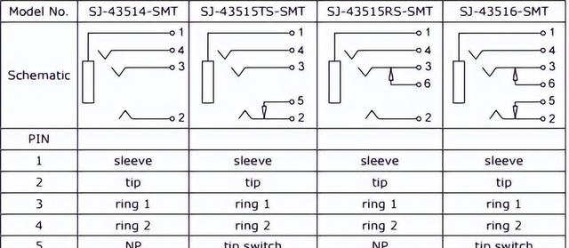
Numbered keys and various types of encapsulations
- Ensure that indicators for all components are present
The main display stop in assembly is missing pin 1 indicator or component polarity/direction indicator on the screen. Nearly 75% of the assembly orders my factory receives fail to identify the location of pin 1 of each IC, or they distort or ignore the polarity that indicates certain capacitors, diodes, or LEDs.
The best way to avoid assembly issues: Negotiate with the PCB factory before the design begins.
Follow the convention for marking diode polarity, including LEDs: put a K on the silkscreen layer at the cathode. Alternatively, use the correct orientation of the diode electrical symbol to guide assembly.
Never indicate diode polarity based on the anode pad. Use K to specify the cathode or arrange the diode symbol in the correct position. Do not substitute any other markings, otherwise the PCB factory will not understand what you mean.
To determine the orientation of the tantalum capacitor, mark the positive electrode with a plus sign on the silkscreen. Keep in mind that tantalum capacitors may ignite if they are installed with swap polarity. Unless the schematic is reverse-engineered, the PCB factory cannot determine the polarity of the part unless it is clearly displayed.
Screen printing must not interfere with the pads and symbols must not be printed under the body of any component.
- Each connection of each component must have its own independent pad
The dimensions of each pad must correspond to its component. If two components share a pad, for example, a resistor and a capacitor, neither will align correctly during assembly.
If a pad is much larger than the pad of one of its components, the component monument may be caused by an imbalance in solder deposition.

Independent pads for each component (from Corecore EMA)
If dumping or flat surfaces will become contact points, there must be appropriately sized mask definition pads. If the device involves non-solder mask-defined pads for connection as well as pads defined by solder masks, a BGA matrix on loosely spaced, for example, some of these adjacent outer balls are shared with ground dumping – it is specified in the design notes that the board PCB factory must not edit the solder mask aperture for the pads defined by these solder masks.
- Material procurement issues
Now many PCB factories are one-stop, PCB board design, material procurement, stencil fixtures, PCB assembly are all together.
But if your components are not all supplied by the PCB factory, you must provide the parts in a well-organized kit that matches the BOM. All SMT components must be supplied as rolls, or in continuous tape at least 6 inches long, or in tubular or pallet form.
Each part number listed on the BOM requires additional components to cover the backup loss during assembly. For example, an assembly shop may need at least 10% or 20% more 0201 1k ohmic resistance than the 0201 1k ohm required on the BOM. The parts of each line item on the BOM must be placed in a clearly marked bag, separate from the other parts.
PCB one-stop vendor loss diagram (from AiPCBA)
All ICs must be shipped in original, unopened, protective packaging containing desiccant.
Finally, the best way to avoid material problems: consult with the PCB factory before the design begins, and one-stop PCBA is also good.
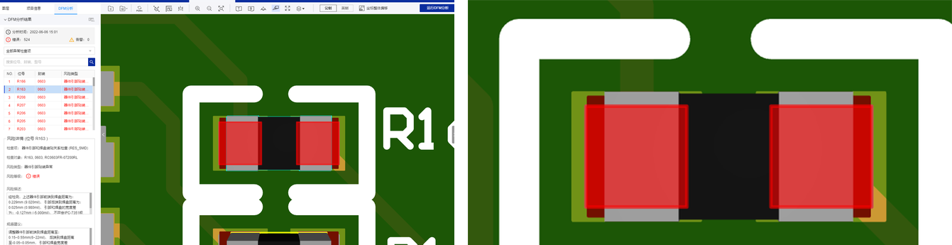
- DFM inspection
An important way to ensure that your PCB is error-free and works seamlessly is to run Design for Manufacturing (DFM) testing. The test identifies any errors in the design at an early stage, avoiding costly errors and delays that have to be dealt with at a later stage. It can identify the spacing between components, component polarity, packaging confirmation and other problems in time.
In addition, DFM testing helps to:
- Reduce expenses
- Accelerate delivery and save time on rework
- Improve product quality