


Introduction
In power supplies, industrial controls, new energy systems, and medical electronics, high-power PCBAs (Printed Circuit Board Assemblies) operate under sustained high-load conditions. Power devices, rectifier modules, inductors, and high-current trace areas become concentrated heat sources. According to industry statistics, approximately 60% of electronic device failures are directly related to temperature anomalies. Excessive localized temperature rise accelerates component aging, reduces solder joint reliability, and can trigger protective shutdowns or even catastrophic burnout. Relying solely on theoretical calculations or traditional contact-based temperature measurement is no longer sufficient to capture the thermal dynamics under real-world operating conditions—this is precisely why infrared thermal imaging analysis has become indispensable in the high-power PCBA manufacturing and validation process.
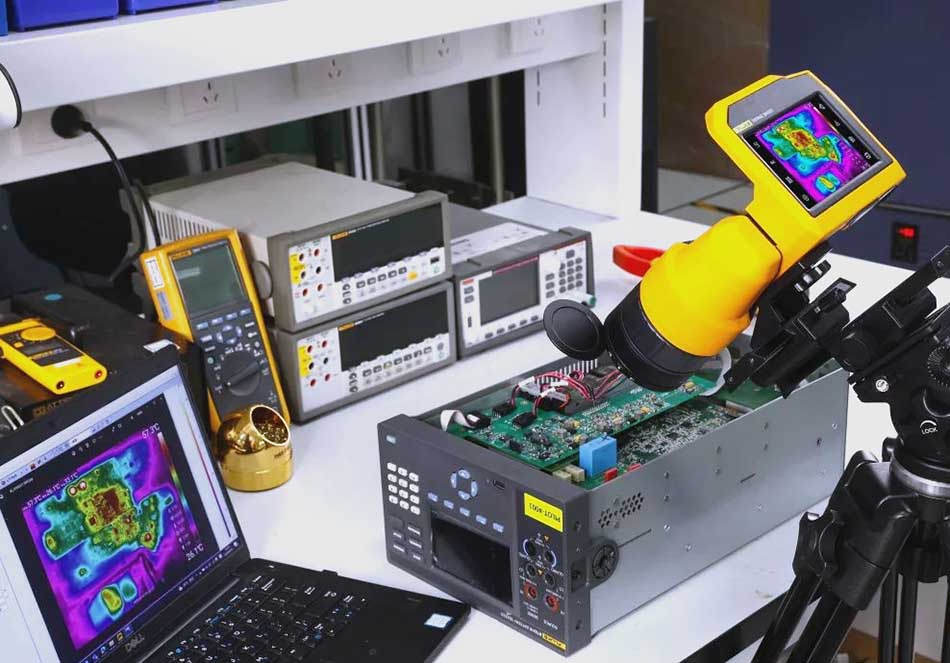
1. Core Value of Infrared Thermal Imaging Analysis
1.1 Non-Contact, Non-Destructive Testing: Safe and Reliable
Infrared thermal imaging captures the infrared radiation emitted from the PCBA surface, converting invisible thermal states into visual images, enabling full-board temperature measurement without physical contact. Compared to traditional contact sensors such as thermocouples, this method eliminates the risk of electrostatic discharge (ESD) damage caused by physical contact and does not alter the thermal field distribution of the components under test. This makes it particularly suitable for dynamic testing of high-density, high-value high-power PCBAs.
1.2 Full-Scene Visual Analysis: Uncovering “Hidden” Problems
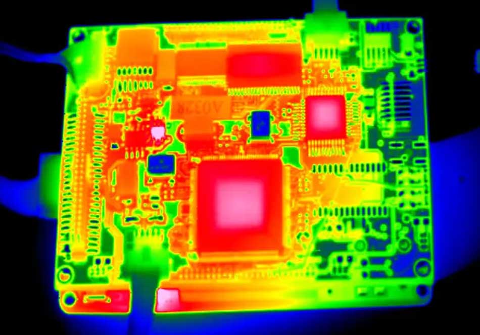
Thermal imaging technology provides real-time visualization of the entire board’s temperature distribution, making high-temperature areas and abnormal temperature differentials immediately apparent. High-sensitivity thermal cameras can detect minute temperature differences as small as 0.03°C to 0.05°C, with resolutions ranging from 320×240 to 1280×1024 pixels, enabling precise localization of everything from millimeter-scale solder joints to high-power MOSFETs. Issues that are difficult to detect through visual inspection or conventional electrical testing—such as poor soldering, inadequate copper foil connections, and excessive component contact resistance—are directly exposed through abnormal temperature rise under load conditions.
1.3 Dynamic Monitoring and Data Traceability
Thermal imaging supports multiple measurement modes including spot, line, and area analysis, generating trend charts, 3D thermal maps, and temperature matrices. When combined with real-time temperature curve analysis and video recording, it provides comprehensive data support for design validation, process qualification, and batch quality assessment.
2. The Critical Role of Infrared Thermal Imaging in Design Validation
2.1 Optimizing Thermal Layout and Reducing Iteration Costs
During the PCB design validation phase, applying rated or loads allows thermal imaging to reveal the actual temperature field and identify “hotspot areas” where temperatures exceed 80% of a component’s rated temperature tolerance. In one case, an initial power PCB design revealed through thermal imaging that the temperature near a MOSFET reached 120°C (rated tolerance: 150°C). After increasing the heat-dissipating copper foil area and adding thermal vias, the hotspot temperature dropped to 95°C, meeting design requirements.
2.2 Comparative Validation of Design Solutions
When evaluating solutions such as current-sharing circuits, heatsink contact quality, and airflow channel design, infrared thermal imaging provides quantitative comparison data. For example, during testing of Texas Instruments’ PMP40909 power converter, engineers used high-resolution thermal cameras to compare thermal distributions with and without current-sharing design. The module with current-sharing circuitry showed more uniform temperature distribution and achieved output power capability exceeding 40W, fully consistent with current measurement results. This case demonstrates that thermal imaging is not only a “see-through eye” but also a “regulator” for design optimization.
2.3 Aiding Component Selection and Layout Decisions
Issues such as excessive dropout voltage in high-power LDOs, insufficient current rating in DC-DC inductors, and poor RF power amplifier matching all lead to abnormal component heating. Thermal cameras can evaluate the thermal characteristics of different components, helping R&D engineers identify the “weak-link effect” during the prototype stage—where overheating of a single component causes premature failure of the entire board—thereby optimizing layout and balancing thermal loads.
3. Applications of Infrared Thermal Imaging in Manufacturing and Quality Control
3.1 Precision Localization of Solder Defects and Process Deviations
In PCBA manufacturing, defects such as insufficient solder paste volume, cold solder joints, and inadequate copper foil connections result in increased contact resistance (>100 mΩ), generating Joule heating under power and appearing as localized hotspots on thermal images (temperatures 15–30°C higher than normal solder joints). During batch sampling of an LED driver board, thermal imaging revealed that 10% of samples exhibited pad hotspots. Investigation confirmed that solder paste volume was only 60% of the design value. After adjusting process parameters, the defect rate dropped to below 0.5%.
3.2 Rapid Diagnosis of Short Circuits and Leakage Faults
Short-circuit faults can generate temperatures exceeding 100°C instantly when power is applied. Thermal cameras can immediately capture and localize such faults, preventing prolonged power application that could burn the PCB. For Faint leakage currents caused by interlayer insulation degradation (temperature rise of 3–5°C), high-sensitivity thermal cameras can effectively identify these issues—faults that are often undetectable with a multimeter. In one case, a communication PCB experienced intermittent network disconnections with no abnormalities found during electrical testing. Thermal imaging captured a sudden 25°C temperature spike (45°C → 70°C) near the network interface chip during fault occurrence, ultimately diagnosing an internal cold solder joint within the chip.
3.3 Supporting SMT Process Temperature Control and Aging Testing
In SMT reflow soldering, wave soldering, and other processes, temperature curve fluctuations directly impact solder joint quality. Infrared thermal cameras enable real-time monitoring of soldering temperature changes, allowing parameter adjustments to improve consistency. In aging and reliability testing, continuous power-on monitoring (e.g., 1000 hours) with temperature recording enables evaluation of material degradation effects on thermal performance, providing early warning of thermal runaway risks. In one new energy battery test, a thermal camera provided a 3-hour advance warning, preventing an explosion accident.
4. TORTAI Technologies’ Practices and Capabilities
As a professional enterprise specializing in high-reliability electronic manufacturing services, TORTAI Technologies (Dongguan Gaotuo Electronics Technology Co., Ltd.) has integrated infrared thermal imaging analysis into its standard PCBA manufacturing verification process. The company is equipped with industrial-grade thermal imaging inspection systems, forming a comprehensive quality control framework alongside SPI, AOI, X-ray, ICT/FCT, and other inspection equipment.
In high-reliability sectors such as medical devices, automotive electronics, and industrial controls, TORTAI strictly adheres to ISO9001, ISO13485, and IATF16949 quality management systems, executing to IPC-A-610J CLASS III standards. Through infrared thermal imaging analysis, we can identify thermal issues before shipment and provide customers with full lifecycle thermal management data support, including:
- Prototype stage:Collaborating with customers to optimize thermal design and component layout;
- Trial production stage:Screening for process defects that cause thermal anomalies;
- Volume production stage:Establishing thermal behavior baselines to ensure product consistency and long-term stable operation.
“The reliability of high-power PCBA often begins with thermal management.” This is the technical philosophy behind TORTAI’s deep integration of infrared thermal imaging into its manufacturing services.
5. Frequently Asked Questions (FAQ)
Q1: Can infrared thermal imaging replace traditional thermocouple temperature measurement?
A: The two methods serve different purposes. Thermocouples are suitable for high-precision contact measurement at single points but cannot cover the entire board and introduce contact interference. Infrared thermal imaging’s irreplaceable value lies in its ability to provide large-area, dynamic, non-contact visualization of the full temperature field. In engineering practice, the two are often used complementarily: thermal imaging for rapid hotspot screening, followed by thermocouples for precise calibration of critical areas.
Q2: How can the accuracy of thermal imaging temperature measurement be ensured?
A: Key considerations include: ① Setting the correct emissivity (different materials have different emissivity values; PCBA surfaces typically use 0.85–0.95); ② Maintaining a stable ambient temperature (23±2°C), avoiding airflow and direct sunlight; ③ Keeping the lens clean and using manual focus mode for close-range inspection to ensure image clarity; ④ Regular calibration of the thermal camera using a blackbody furnace.
Q3: Is infrared thermal imaging applicable to all types of PCBA faults?
A: It is primarily applicable to faults related to temperature changes, such as overheating, poor heat dissipation, short circuits, cold solder joints, poor contact, and uneven load distribution. For faults that do not generate significant temperature rise (e.g., pure logic errors, signal integrity noise), it must be combined with ICT, FCT, oscilloscopes, and other tools for comprehensive troubleshooting.
Q4: How long does a PCBA need to be powered on before thermal imaging analysis?
A: This depends on the product’s thermal time constant. It is generally recommended to operate until thermal equilibrium is reached (temperature change < 2°C over 5 minutes), typically requiring 5 to 30 minutes. For fault localization, a step-loading method can be used: starting from 50% load and gradually increasing to 120%, observing the emergence trend of abnormal temperature points to avoid overload damage to sensitive components.
Q5: As a PCBA procurement party, how can I evaluate a contract manufacturer’s thermal imaging capability?
A: Focus on three aspects: ① Whether they are equipped with professional-grade thermal cameras (resolution ≥ 320×240, thermal sensitivity ≤ 50 mK); ② Whether they have standard thermal imaging inspection work instructions and record traceability systems; ③ Whether they can provide thermal simulation analysis or measured data support during the DFM stage to help optimize design. TORTAI Technologies’ thermal imaging inspection system is integrated into the MES, enabling thermal data traceability for each individual PCBA.
Conclusion
Infrared thermal imaging analysis has evolved from a development support tool into a “standard configuration” for PCBA full-lifecycle quality management. It not only helps engineers discover “visible defects” during the design and production phases but, more importantly, drives improvements in thermal dissipation structures, process parameter adjustments, and continuous reliability enhancement through quantified thermal distribution data.
For high-power PCBA, every thermal imaging test represents a deep validation of product stability. If you are facing challenges with abnormal temperature rise, thermal bottlenecks, or PCBA quality improvement needs, consider incorporating infrared thermal imaging analysis into your verification process—as TORTAI Technologies advocates: driven by data for thermal management, safeguarding product vitality with expertise.