


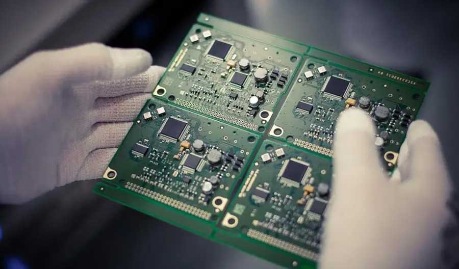
As electronic products continue to evolve towards miniaturization, lightweight design, and higher performance, microelectronics packaging technology has become a crucial element in PCBA (Printed Circuit Board Assembly) processing. This technology not only influences the performance and reliability of the circuit board but also directly impacts the overall quality and lifespan of the final product.

1、Overview of Microelectronics Packaging Technology
Microelectronics packaging refers to the process of encapsulating semiconductor chips and electronic components onto a circuit board to achieve electrical connection, mechanical protection, and thermal dissipation. In the context of PCBA processing, packaging technologies can be broadly categorized into traditional and advanced packaging:
- Traditional Packaging: Examples include DIP (Double In-line Package) and SOP (Small Outline Package). These are suitable for relatively simple electronic products.
- Advanced Packaging: Technologies such as BGA (Ball Grid Array), QFN (Quad Flat No-lead), and CSP (Chip Size Package) meet the packaging requirements for high-density, high-performance components. They are widely used in fields like smartphones and automotive electronics.
The advancement of microelectronics packaging technology provides essential support for PCBA factories to enhance product performance and reduce size.
2、Major Types of Microelectronics Packaging Technology
In PCBA processing, common microelectronics packaging technologies include the following:
BGA (Ball Grid Array) Packaging Technology
BGA is a high-density packaging technology primarily used for chips with a high pin count. Its advantages include improved heat dissipation and electrical connection stability for components, making it suitable for complex electronic devices. It is widely used in high-end products like computer motherboards and communication equipment.
QFN (Quad Flat No-lead) Packaging Technology
QFN is a compact packaging type suitable for miniaturized products. Its strengths lie in its thin profile, small size, superior electrical performance, and ease of heat dissipation. It finds extensive application in mobile devices, medical electronics, and similar fields.
CSP (Chip Size Package) Packaging Technology
CSP is a packaging technology where the package size is very close to the die itself, significantly reducing the space required for encapsulation. Its key advantage is miniaturization, making it ideal for high-density PCB design. It is primarily used in micro-electronics like smartphones and wearable devices.
SIP (System-in-Package) Technology
SiP integrates multiple chips into a single package to achieve higher system functionality integration. It offers the benefits of space savings and performance enhancement, making it suitable for multifunctional products. It is widely applied in high-end areas such as IoT (Internet of Things) and 5G communication equipment.
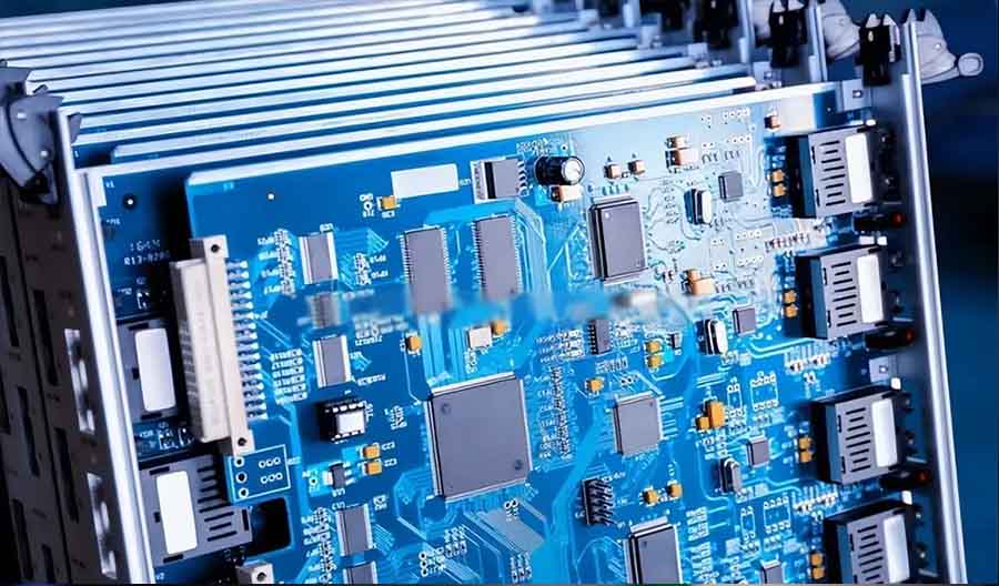
3、Impact of Microelectronics Packaging Technology on PCBA Processing
The continuous development of microelectronics packaging technology imposes higher demands on the production techniques and processes of PCBA factories:
3.1 Enhancing Precision in PCBA Processing
Advanced packaging technologies require higher placement accuracy and soldering quality. PCBA factories need to introduce high-precision placement equipment and soldering technologies to ensure the stability and reliability of packaged components.
3.2 Driving Process Upgrades
Microelectronics packaging places greater demands on temperature control and material selection. This drives PCBA factories to continuously optimize process flows such as reflow soldering and selective soldering, thereby improving overall production standards.
3.3 Strengthening Quality Inspection and Control
Within microelectronics packaging, the inspection of hidden solder joints and high-density soldering becomes more challenging. PCBA factories need to adopt advanced equipment like AOI (Automated Optical Inspection) and X-Ray inspection to ensure high-quality output throughout the manufacturing process.
4、Future Development Trends in Microelectronics Packaging Technology
In response to the constant iteration of electronic products, microelectronics packaging technology continues to innovate, primarily showing the following trends:
- Higher Density, Smaller Packages: To meet the needs of device miniaturization and increase the integration level of circuit boards.
- Enhanced Thermal Performance: Improving the heat dissipation capability of components by optimizing packaging materials and structural design.
- Multi-chip Integration: Utilizing technologies like SiP to integrate various functions into a single package, boosting product performance.
- Automated and Intelligent Production: PCBA factories will further increase the automation level of packaging technology to achieve efficient and precise production.
Summary
Microelectronics packaging technology is one of the core technologies in PCBA processing, playing a vital role in the miniaturization and high-performance evolution of electronic products. Tortai Technologies has consistently addressed market demands by introducing advanced packaging technologies, optimizing process flows, and enhancing inspection capabilities to provide high-quality electronic manufacturing services for clients. In the future, with the ongoing development of technology, microelectronics packaging will bring more innovation and development opportunities to the PCBA processing industry.