


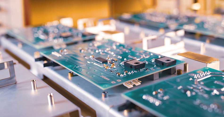
In the PCBA manufacturing process, the silkscreen markings on components serve not only to convey part numbers, polarity, and revision status but also play a crucial role in SMT placement, automated optical inspection, and downstream maintenance workflows. During the product design phase, engineering teams often prioritize electrical performance and signal integrity while overlooking the governance of silkscreen orientation consistency. In practice, inconsistent silkscreen orientation leads to increased complexity in pick-and-place programming, higher false-reject rates in inspection systems, and introduces a range of latent engineering risks throughout volume production and the full product lifecycle.
1、The Coupling Mechanism Between Silkscreen Orientation and SMT Placement Efficiency
During pick-and-place programming and vision alignment, the directional parameters of component silkscreen directly influence the preset pickup angles and rotational compensation strategies. If identical components are presented on the PCB surface with non-uniform silkscreen orientations, the placement program must independently define angular offsets and nozzle rotation paths for each discrete pose. This not only increases the engineering time required for program generation and optimization but also introduces redundant motion control commands during high-speed placement, thereby extending the cycle time per board. For PCBA projects with production volumes reaching tens of thousands of units, the cumulative effect of this minor variance significantly inflates manufacturing costs and erodes overall line utilization rates.
2、Impact on AOI and SPI System Recognition Accuracy
Modern PCBA lines heavily rely on Automated Optical Inspection (AOI) and Solder Paste Inspection (SPI) systems for closed-loop process control. At the algorithmic level, these systems frequently utilize silkscreen edges or character features as fiducial references for image registration and polarity verification. When silkscreen orientations are disordered, the template matching success rate of machine vision algorithms drops substantially, manifesting as a simultaneous increase in False Call rates and Escape Rates. Even with the introduction of secondary manual verification, this results in increased inspection labor per unit area and a higher incidence of rework due to human error, directly compromising the reliability and cost-effectiveness of the inspection stage.
3、Assurance of Rework Efficiency and Product Traceability
During post-delivery maintenance and failure analysis, uniformly oriented silkscreen provides field engineers with intuitive visual guidance, enabling rapid identification of target devices and confirmation of polarity, thereby effectively mitigating the risk of secondary damage caused by polarity misjudgment. Conversely, haphazard silkscreen orientation forces maintenance personnel to cross-reference schematic diagrams repeatedly to verify physical location and direction, substantially increasing troubleshooting time. Particularly on high-complexity boards, this significantly elevates the potential for repair errors, thereby threatening the long-term reliability of the system and the quality of after-sales service.
4、Layout Constraints in High-Density Interconnect (HDI) Boards
With the industry trend toward high-density assembly and miniaturization, available surface space for silkscreen on the PCB is extremely constrained. Unregulated silkscreen orientation can lead to character overlap, obstruction of test points, or interference with the visual inspection of fine-pitch component solder joints. Planning clear, uniformly oriented silkscreen areas at the design stage is not only an adherence to Design for Manufacturing (DFM) principles but also a critical prerequisite for ensuring ICT probe accessibility and the efficiency of manual visual inspection.
5、Collaborative Design Specifications Between Design and Manufacturing
Consistency in silkscreen orientation is not a remedial action to be taken during manufacturing; rather, it must be established upfront within the EDA design flow. PCB layout specifications should explicitly define the orientation reference for all polarized components (e.g., uniformly facing the board edge or a specific quadrant). Furthermore, design reviews should achieve closed-loop confirmation with the PCBA service provider regarding placement rotation rules and inspection program parameters. This design-process collaboration mechanism systematically enhances production line throughput and first-pass yield without incurring additional hardware costs.
6、The Leverage Effect of Minor Process Specifications on Overall Quality
The unification of component silkscreen orientation may appear to be a minor cosmetic process requirement; however, it is, in fact, a critical engineering detail control metric that spans R&D design, SMT manufacturing, automated inspection, and backend repair. It reflects a project team’s profound understanding of Design for Manufacturing and Lean Production principles and serves as a key lever for enhancing the comprehensive quality and total lifecycle value of PCBA products.
If your project encounters placement efficiency bottlenecks, frequent AOI false calls, or excessive rework hours during PCBA prototyping or mass production, we recommend investigating the standardization of silkscreen orientation controls. We can provide comprehensive technical support ranging from DFM specification development to full-scale production implementation, assisting you in achieving global consistency management of silkscreen markings throughout the PCBA process.