


In the final sprint of electronic product development, a failed PCBA prototype can feel like a sudden storm, scattering project budgets and potentially slamming shut the critical window to market. Understanding the systemic root causes behind these failures is the first line of defense in building product success.
In the increasingly competitive field of electronic manufacturing, PCBA prototyping serves as the crucial bridge between design and mass production. Its success or failure directly determines whether a product can smoothly enter the market. However, industry data suggests that up to 65% of circuit board faults originate from design flaws or process violations. Each prototype failure means delays in the R&D cycle, cost overruns, and a blow to team morale. More critically, many issues latent during the prototyping phase, if not detected and corrected in time, can trigger disastrous batch failures and recall risks during mass production. This article, integrating the latest industry practices and case studies, provides an in-depth analysis of the seven primary causes leading to PCBA prototype failure and offers systematic avoidance strategies based on industry standards. The aim is to help R&D teams transform the prototyping phase from a “problem exposure field” into a “success verification field.”
1、Design Flaws: “Suicidal” Layout and Routing That Violates Rules
Design is the DNA of a PCBA. Many catastrophic failures at the prototype stage have their roots buried deep in the drawing phase. The most common fatal errors concentrate on violating fundamental design rules.
Primary Cause: Violating Trace Width/Spacing and Thermal Management Design
According to the IPC-2221 standard, trace width/spacing for industrial-grade products should be no less than 0.2mm. However, in pursuit of high density, many engineers engage in “suicidal routing,” using traces below 0.1mm. This directly leads to uncontrolled impedance (error exceeding ±15%) and increases the risk of short circuits by 3.8 times. In industrial control equipment, high-power loads like motor drivers and relays generate large currents. If the power and ground trace widths are insufficient (recommended ≥50 mils), severe heating or even board burn-out can occur due to excessive line resistance. Simultaneously, the lack of thermal design under high-power components (e.g., MOSFETs)—such as not laying sufficiently thick thermal copper pours (≥2 oz) or optimizing thermal via layouts—can cause component overheating and failure.
Case Study
An industrial control device experienced frequent MCU resets during prototype testing. Investigation revealed the root cause was not a software bug, but a power trace to the MCU that was only 0.15mm wide and excessively long. When peripheral circuits activated, the current surge caused a significant voltage drop on this line, triggering the MCU’s undervoltage protection. The solution involved recalculating and widening the critical power path according to IPC standards and minimizing its length. This case demonstrates that neglecting basic design rules directly leads to core functional failures.
How to Avoid
- Adhere to Standards: Treat design standards like IPC-2221 as the “constitution” for routing. Use trace width calculators to verify the current-carrying capacity of all high-current paths.
- Simulation First: Utilize simulation software (e.g., Flotherm) to model thermal distribution and power integrity before releasing boards for fabrication, identifying overheating and voltage drop risks early.
- Build in Redundancy: For high-speed signals and critical power lines, incorporate a 10% width redundancy during the design phase to accommodate process variations.

2、Component Selection and Management Errors: The “Hidden Reefs” of the Supply Chain
Improper component selection and management is another high-frequency minefield for prototype failure. It’s not just a matter of “what to choose,” but also “how to ensure” reliability and availability.
Primary Cause: Grade Mismatch and Lack of Traceability
Using consumer-grade components in harsh industrial environments poses a significant risk. Consumer-grade parts have large parameter drift over temperature; within a wide temperature range (e.g., -40°C to 85°C), this can lead to severe performance shifts. For instance, a device failed to start at low temperatures because a consumer-grade capacitor lost 30% of its capacitance. On the other hand, many prototype projects neglect component traceability management. Failing to require suppliers to provide complete RoHS, REACH certifications, and lot/batch numbers creates a predicament if defects arise—problems cannot be traced back to their source quickly to contain affected batches.
Case Study
A company developing an outdoor IoT device found its prototype functionally perfect. However, during temperature cycling tests (-40°C to 85°C), the device frequently locked up at high temperatures. After extensive troubleshooting, the root cause was identified as a commercial-grade LDO regulator chip (rated 0°C to 70°C) chosen for its low cost, which degraded severely at high temperatures. Replacing it with an industrial-grade, wide-temperature chip (-40°C to 125°C) resolved the issue. This case highlights the cost of ignoring component operating temperature grades.
How to Avoid
- Select Grades Strictly: Clearly define the product’s operating environment requirements and mandate the use of industrial-grade or automotive-grade wide-temperature components, verifying detailed specifications in their datasheets.
- Manage the Supply Chain: Establish an Approved Vendor List (AVL). For critical components (e.g., MCUs, power ICs), prepare at least two alternative, compatibility-tested part numbers to mitigate shortage risks.
- Build a Traceability System: From the prototype stage, request and record the lot/batch number for every critical component. Create a simple traceability log to lay the groundwork for future failure analysis.

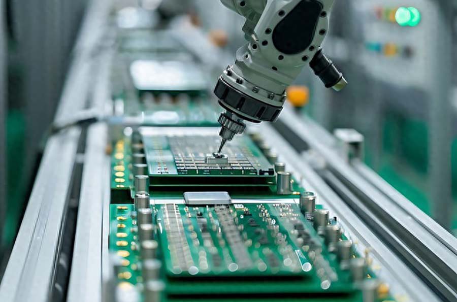
3、Soldering Process and Assembly Reliability: The “Fragile Link” of Connections
Soldering is the physical process that turns design into reality. Uncontrolled process parameters in this phase are a direct trigger for prototype functional failures.
Primary Cause: BGA/QFN Soldering Defects and Process Variability
Components like BGAs and QFNs pose high soldering quality risks due to their hidden solder joints. Issues like cold solder joints, voids, and bridging are frequent during prototyping. For example, intermittent device lock-ups were traced back to a BGA cold solder joint, only detectable via X-Ray inspection. Furthermore, non-standardized soldering process parameters are another trap. If parameters like stencil aperture dimensions and reflow profiles from the prototype phase are not meticulously documented and locked down, significant variation can occur during transition to mass production, causing yield to plummet. One project saw a 15% yield drop in production because of an undocumented change to stencil aperture size, leading to insufficient solder paste volume.
Case Study
A key video processing chip on a smart hardware mainboard used a QFN package. The prototype passed lab tests, but during pilot production, 30% of units exhibited screen corruption. Analysis revealed an improperly set preheat ramp rate in the reflow oven, preventing the solder under the chip’s large central thermal pad from fully melting, resulting in a large-area cold solder joint. Adjusting the temperature profile to extend time above liquidus solved the problem.
How to Avoid
- Mandatory Inspection: For all BGA and QFN packages, enforce X-Ray inspection at the prototype stage to ensure the absence of voids, bridging, and other defects.
- Freeze the Process: Upon successful prototype verification, immediately document and “freeze” all process parameters—stencil files, placement programs, reflow profiles—as the golden standard for production.
- Evaluate New Processes: For high-density boards, evaluate new processes like selective wave soldering or laser soldering to improve the reliability of soldering special components.
4、Inadequate Test Coverage and Missing Environmental Validation: The Distorted “Safe Zone”
A prototype passing tests in a “benign” lab environment doesn’t guarantee it can withstand real-world conditions. Insufficient testing is a primary reason for “false success” in prototypes.
Primary Cause: Disconnect Between Test Scenarios and Real Environments
Many Functional Circuit Tests (FCT) are conducted only under no-load or ideal conditions, failing to simulate complex real-world operational scenarios like loaded operation, temperature variation, or vibration. A device functioning normally in the lab but failing in the field due to connector loosening from mechanical vibration is a classic case of inadequate test coverage. Simultaneously, completely overlooking Environmental Stress Screening (ESS) is a fatal error. Without tests like temperature cycling or thermal shock, components with latent defects or poor environmental endurance cannot be screened out.
Case Study
A PCBA for a smart home Bluetooth speaker delivered perfect sound quality during prototype listening tests. However, when the first batch shipped to humid southern regions, a significant number exhibited no sound or loud noise on power-up. Failure analysis revealed that surface-mount inductors on the mainboard, lacking conformal coating, absorbed moisture in the humid environment, causing inductance drift and failure of the audio filter circuit. This issue could have been exposed earlier had an “85/85” test (85°C/85% humidity) been performed during prototyping.
How to Avoid
- Simulate Real-World Testing: Develop test fixtures that simulate real loads and operational scenarios, subjecting the prototype to electrical stresses akin to real application.
- Implement Environmental Stress Screening: Perform at least basic ESS on prototypes, such as temperature cycling (e.g., -40°C to 85°C) and high-temperature/high-humidity testing, to precipitate potential defects early.
- Conduct EMC Pre-compliance Testing: Perform basic EMC pre-tests (e.g., ESD, surge) during the R&D phase to avoid show-stopping issues during formal certification.

5、Mechanical and Protective Design Flaws in PCBA: The Overlooked “Physical World”
A PCBA must not only be electrically correct but also physically suited to its assembly and operating environment; otherwise, installation failure or early physical damage will occur.
Primary Cause: Poor Design for Assembly (DFA) and Lack of Environmental Protection
Failing to consider mechanical features like tooling edges, fiducial marks, and mounting hole locations during design can prevent the PCBA from being installed or securely fastened within the enclosure. For instance, missing or misaligned fiducial marks can cause misalignment during SMT placement and subsequent assembly. More critically, neglecting protective design for the operating environment is a severe oversight. In damp, dusty industrial settings, the failure rate of an unprotected PCBA can multiply. Case studies show that applying conformal coating compliant with IPC-CC-830B can reduce device failure rates in humid environments by up to 80%.
Case Study
The PCBA prototype for an industrial sensor module functioned correctly during bare-board testing. However, after being installed into its metal housing and screws tightened, some units lost communication. Investigation found that a critical crystal oscillator was placed directly under a mounting post. Tightening the housing induced slight PCB bending, placing excessive stress on the oscillator and causing it to stop. This is a classic case of insufficient consideration for Design for Manufacturability (DFM) and Design for Assembly (DFA).
How to Avoid
- Review Mechanical Drawings: Upon completing PCB layout, separately review its mechanical drawing to ensure fiducials, mounting holes, keep-out areas, etc., meet final assembly requirements.
- Apply Protective Processes: Based on the product’s application environment, evaluate and finalize the conformal coating process (spray, dip, etc.) during prototyping and verify its effectiveness.
- Perform Cleaning Validation: For high-reliability products, implement rigorous cleaning to remove flux residues (preventing ionic migration) and avoid using corrosive solvents.

6、Supply Chain Communication and Document Handover Gaps: The Cost of Information “Silos”
Sometimes, prototype failure isn’t a technical issue but a management problem caused by distorted or broken information flow.
Primary Cause: Incomplete Design Files and Inefficient Communication
Providing incomplete or ambiguous files to the manufacturer is a direct cause of incorrect prototypes. Examples include missing accurate assembly drawings, confused BOM versions, or incorrect Gerber layer assignments. Furthermore, a lack of proactive, in-depth communication between the R&D team and the manufacturer—relying solely on email for file transfer—without sufficiently confirming process details (like soldering temperature for special components or assembly sequence for shields) leads the manufacturer to proceed based on “standard practice,” often resulting in deviations.
Case Study
An R&D team designed a PCBA with an RF module, specifying a shield can part number in the BOM. However, the assembly drawing failed to clarify the attachment method (solder vs. conductive adhesive) and grounding point locations. The manufacturer performed standard SMT soldering. The returned prototypes fell far short of RF performance targets. Troubleshooting revealed poor shield grounding severely degraded shielding effectiveness. Updating the assembly drawing with clear Craftsmanship requirements resolved the issue.
How to Avoid
- Standardize Files and Control Versions: Establish a standardized package checklist including Gerber, BOM, assembly drawings, and process notes. Implement strict version control for all files (e.g., V1.2.3_PCB).
- Front-load Communication and On-site Audit: Hold a technical alignment meeting with the manufacturer’s key process engineers before prototyping to confirm all special requirements. Conduct on-site audits if possible.
- Establish a Feedback Loop: Upon receiving prototypes, inspect them not only for function but also from a manufacturing quality perspective. Feed any discrepancies back to the manufacturer to form a continuous improvement loop.

7、Lack of Systematic Verification and Iteration Process: The Illusion of “First-Pass Success”
Banking on prototype success with a “get it right the first time” mentality, without planning for iteration and validation, is the greatest risk in project management.
Primary Cause: Skipping Pilot Run and Jumping Straight to Mass Production
Many teams, after their first prototype (maybe just 5-10 pieces) passes functional tests, rush into mass production of hundreds or thousands of units. This bypasses the critical Pilot Run or Pilot Volume Testing (PVT) phase. The purpose of PVT (typically 50-100 pieces) is to validate supply chain stability and process consistency, not just the design itself. Projects have been derailed precisely because they skipped this step, discovering during mass production that a secondary source for a component had unreliable lead times, completely disrupting the production schedule.
Case Study
A startup developed an innovative medical diagnostic device. The first Engineering Verification Test (EVT) units (3 pieces) performed brilliantly in clinical demos. Confident, the team placed an order for 500 sets directly. The first 100 units produced had over a 30% failure rate during calibration. Emergency investigation revealed that a precision resistor used in the prototype was a high-grade “milspec” sample an engineer sourced from the lab, with exceptional performance. The commercially procured, same-part-number resistors for mass production had far greater temperature drift and tolerance dispersion than expected, causing system reference voltage drift. A 50-unit pilot run would have certainly exposed this issue beforehand.
How to Avoid
- Plan for Multiple Iterations: Explicitly plan for at least two or more prototype iterations (EVT, DVT) in the project schedule, allocating time for design revisions.
- Mandate a Pilot Run: Establish a small-batch pilot run (50-100 pcs) as a mandatory gate before full-scale production, to validate the supply chain, process stability, and test fixture reliability.
- Create a “Golden Sample” Archive: Archive the final approved prototype along with all its test data and process parameter documents as a baseline for production comparison and failure analysis.
Conclusion
PCBA prototype failure is rarely due to a single,By chance factor. It is often the concentrated manifestation of oversights across multiple links: design, components, process, testing, and management. The key to avoiding failure lies in establishing a systematic, prevention-oriented R&D process that shifts quality control checkpoints significantly forward from “post-facto inspection” to “preventive design” and “in-process control.” This requires engineers to think beyond circuit design, embracing a systems mindset encompassing manufacturing, testing, supply chain, and reliability.
Every successful prototype validates this systems thinking. Every failure should become valuable input for optimizing this system. In today’s pursuit of rapid iteration, the ability to “get it right the first time” is more crucial than simply “doing it fast.” This not only saves cost and time but builds the cornerstone for long-term product reliability and market competitiveness.
Tortai Technologies has accumulated profound experience supporting customers with New Product Introduction (NPI) and PCBA prototyping. We deeply understand that a successful prototype is a microcosm of project success. Our engineering team not only provides high-precision manufacturing services but also excels in early engagement. We offer full-process collaborative support—from Design for Manufacturability (DFM) review and supply chain risk Early warning to multi-dimensional reliability validation. We are committed to being an extension of our clients’ R&D teams. Through professional expertise and rigorous processes, we work together to minimize potential risks at the prototype stage, helping innovative ideas transform more robustly and efficiently into mature, reliable products to seize market opportunities.