


1、 Why Do Solder Joints That “Look Fine” Still Fail?
In SMT or through-hole wave soldering processes, solder joint quality is often assessed via AOI (Automated Optical Inspection) or X-ray sampling. Solder joints appearing, with no bridging, are easily deemed acceptable. However, for components like power MOSFETs, DC-DC power modules, and IGBTs, internal solder voids can be a latent failure source.
Voids are bubbles or pores formed by gases (flux volatiles, moisture, trapped air) being trapped during solder melting and solidification. A few small voids may not cause immediate issues. However, when the total void area occupies a significant percentage of the joint interface, or when voids cluster along critical thermal paths, they significantly increase thermal resistance, leading to localized overheating and solder joint fatigue cracking.
2、Principle and Impact Mechanism
Thermal Resistance Increase Principle
The junction-to-case thermal resistance (Rθjc) of a power device consists of the path from the die junction through the solder layer to the substrate/heat sink. Voids within the solder layer cause:
- Reduced effective thermal conduction area → Increased local heat flux density.
- Creation of thermally insulating “air gaps” (Air ≈ 0.026 W/m·K vs. SnAgCu solder ≈ 50-60 W/m·K).
- Result: Increased Rθjc, causing junction temperature (Tj) to exceed specifications under high load, accelerating aging or causing direct thermal failure.
Simplified Empirical Formula:
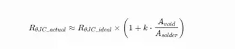
where `Avoid / Asolder` is the void area ratio, and `k` depends on void location and distribution (k is larger on primary thermal paths).
Thermal/Power Cycling Failure Modes
- CTE Mismatch: Stress concentrates around voids during repeated thermal expansion/contraction, easily initiating cracks.
- Accelerated Fatigue: Voids reduce the effective load-bearing area, increasing crack propagation rate.
- Final Manifestation: Solder joint opens or thermal resistance spikes dramatically, causing device failure.
3、Real Case Study & Data Comparison
Case Background
An industrial power supply manufacturer developed a 600W DC-DC module using TO-263 packaged MOSFETs. In the first pilot run of 100 units, all passed initial thermal tests. However, after 500 thermal cycles (-40°C to +85°C), 7 units exhibited power drop and entered shutdown protection.
Investigation & Analysis
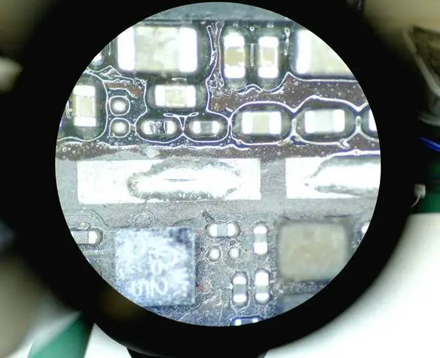
- X-ray Inspection: Failed modules showed average voiding of 22% under MOSFETs, concentrated under the central die (thermal path). Good modules had <6% voiding, evenly dispersed.
- Thermal Imaging: Failed modules showed MOSFET Tj 18°C higher than design, peaking at 128°C (spec ≤110°C).
- Cross-sectioning: Voids caused ~35% increase in local thermal resistance. Through-thickness cracks developed in the solder layer under power cycling stress.
Comparison Data
| Group | Average Void Rate | Thermal Resistance Increase | Failure Rate after 500 Cycles |
| Before Optimization | 22% | +35% | 7% |
| After Optimization | 5% | +6% | 0% |
4、Common Process Control Pitfalls for Engineers
Pitfall 1: Relying Solely on AOI Appearance, Skipping X-ray Sampling
AOI cannot detect internal voids. Power devices require X-ray inspection per a sampling plan (recommended ≥5% or 100% for critical components).
Pitfall 2: Blindly Following Standard Stencil Aperture Recommendations, Ignoring Device Thermal Properties
Power MOSFETs often require increased solder paste deposit area or stepped stencils to ensure sufficient solder fill and reduce space for void formation.
Pitfall 3: Pursuit of Excessively “Fast Ramp-Up” in Reflow Profile
Too rapid heating causes violent, instantaneous flux volatilization, trapping gases before they can escape. Use a gentle preheat/soak stage (e.g., 60-90s at 150–180°C) to allow gradual outgassing.
Pitfall 4: Neglecting PCB Pad Design Impact on Voiding
Micro-gaps, oxidation, or contamination between pads and component leads increase voiding risk. Strictly control Pad surface finish (ENIG/OSP) quality and cleanliness.
Pitfall 5: Omitting First-Article Thermal Testing in Production
The thermal impact of voids may not be apparent at room temperature. Monitoring junction temperature under maximum load during thermal testing is essential for early detection.
5、Engineering Countermeasures & Checklist
Design Stage
- Consider thermal path and pad layout during component selection; prioritize low thermal resistance packages.
- Stencil Aperture Optimization: For power devices, increase aperture area by 10–20% or use local stencil thickening.
- Select oxidation-resistant Pad finishes like ENIG; avoid OSP in high-humidity environments where oxidation risk is higher.
Process Stage
- Reflow Profile: Use a slow, controlled ramp-up during preheat; keep peak temperature and time above liquidus within the midpoint of specification.
- Use low-volatility, low-residue solder pastes (suited for power devices).
- Consider nitrogen atmosphere reflow (optional) to reduce solder oxidation and voiding.
Inspection & Validation
- Perform first-article X-ray inspection targeting voiding (Aim: ≤10% general, ≤5% for critical components).
- Conduct thermal testing to verify junction temperature deviation from design is ≤5°C.
- Perform reliability qualification: Compare voiding percentage and thermal resistance before/after thermal/power cycling tests.
Pre-Production Checklist (Mandatory)
- Stencil aperture design matches component thermal requirements.
- Reflow profile verified via thermal simulation/modeling.
- First-article X-ray inspection completed and recorded.
- Thermal testing covers maximum load conditions.
- Critical component suppliers have provided recommended soldering process windows.
6、Conclusion
Solder voiding is a hidden yet high-risk issue in power PCBA manufacturing. Engineers relying solely on visual inspection or default standard parameters are highly susceptible to thermal failures and batch rework during mass production.
Effective control requires a holistic approach across the entire chain: “Design (Pad, Stencil) → Process (Profile, Atmosphere) → Inspection (X-ray, Thermal Test) → Validation (Reliability).” Furthermore, establishing a correlation database between voiding percentage and thermal performance early in the project lifecycle is crucial for maintaining reliability in high-speed/high-power products.
7、Extended Perspective – Reliability Assurance from Design to Mass Production
Controlling solder voids relies not only on precise design and process parameter settings but also on stable process capability and full-process quality monitoring during pilot runs and mass production. In high-power PCBA manufacturing, even with optimized designs, fluctuations in any stage—stencil fabrication, printing, reflow, or inspection—can cause voiding to re-emerge, compromising product reliability.