一、Drilling
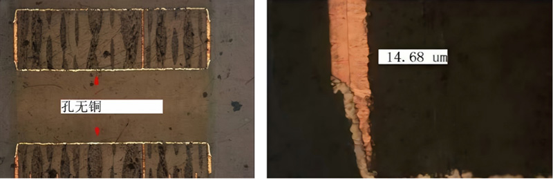
1、Drilling roughness caused by the hole without copper (IPC standard double-sided board 30 microns, multilayer board 25.4 microns).
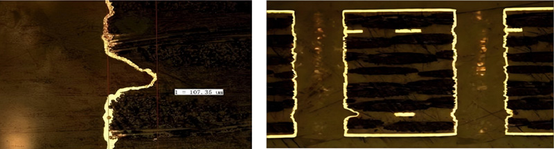
2、Drilling phi caused by hole diameter becomes small / plug holes / acid etching broken holes.

3、Broken drilling nozzles cause holes without copper.

4、Dust plugging holes: mostly generated in the position of the row of holes.

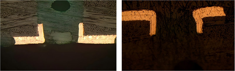
5、The resin and bottom copper at the hole is not completely cut off.

二、Immersed copper plate plating
1、Copper-immersed bubble-type holes without copper, disconnect the location of the hole in the middle and symmetrical, graphic plating layer wrapped in full-plate plating layer
2、Copper-immersed copper backlighting bad type holes without copper: holes in the glass fibre on the intermittent, point-like holes without copper, graphic plating layer wrapped around the whole board plating layer.
3、Unsinking copper plating type holes without copper: only one layer of plating on the surface, no copper in the holes, plating layer wrapped around the substrate copper.

三、Outer layer graphics
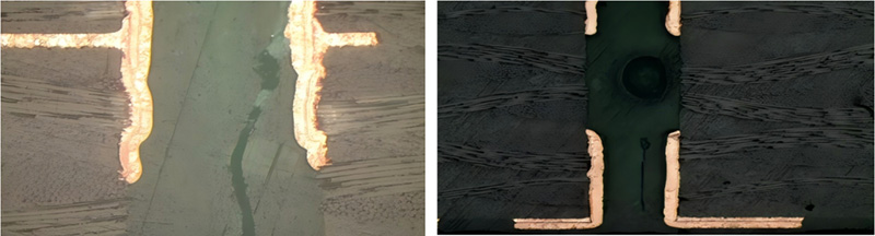
1、Copper breakage at the edge of the aperture, broken copper surface neatly, the graphic plating layer is not wrapped around the whole plate plating layer, caused by the dry film resist into the hole.

2、Dry film plugging holes caused by no copper holes, broken copper surface is neat, the graphic plating layer does not wrap the whole board plating layer.
3、Line pre-treatment volcanic ash plug holes.

4、The outer layer of the line development is not clean, resulting in no copper holes: non-independent holes RING ring is occluded or graphic plating layer and the whole board plating layer between the foreign matter.

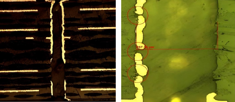
5、Negative plate dry film broken holes: poor exposure or scratch dry film caused by no copper from the mouth of the holes or holes in the copper was bitten thin to the majority of large holes (two full-board plating when the second full-board plating is not wrapped in the first full-board plating).

四、Plating
Tin-plated bubble holes without copper: the main feature is located in the middle of the hole, the break is slope-like, graphic plating layer is not wrapped in full-board plating layer, mostly small holes.

五、Soldermask
Ink plug hole type holes without copper: ink plug holes in the hole hidden micro-etching potion to the hole copper bite thin or bite off.

六、Surface treatment Surface treatment
Large holes, small holes are no copper or copper thickness is insufficient, the board surface green oil under the copper plating layer is complete but exposed copper area copper layer is thin; belong to the micro-etching excessive holes without copper, when there is a slight lack of copper holes, when there is no copper; precipitation of nickel-gold, OSP, spraying, tin, tin and other pre-treatment is excessive.