


Problem Background and Objectives
With the increasing precision and complexity of electronic information products, new challenges and difficulties are posed for the design, fabrication of PCBs, and the assembly of PCBA. In our daily work, the lack of a quantitative assessment for PCB and PCBA makes it difficult to distinguish between ordinary and complex designs, and to determine the appropriate methods for handling them.

Based on these considerations, and referencing existing practices in the industry, we have designed a process complexity calculation formula for PCB and PCBA to address this issue. On another front, targeted efforts have been made in engineering capabilities to achieve the goal of high quality and low cost.
Characteristics of High-Complexity PCBs
From our specific context, high-complexity PCBs exhibit the following characteristics: large dimensions, high layer count (above 18 layers), HDI designs such as 1+10+1 or even 1+16+1, dense line width/spacing (e.g., 3/3, 3/4, 4/4 mil), high aspect ratio for holes (e.g., above 10:1, up to 13.5:1), and the adoption of new surface finishes (such as Immersion Tin, Immersion Silver). Such boards are defined as high-complexity PCBs.
Quantification of PCB Complexity
Therefore, we currently define a high-complexity PCB by four conditions:
- Layer count > 18 (or >20 for backplanes);
- Incorporation of special processes such as HDI, mechanically drilled buried/blind vias, embedded planar capacitors, or back-drilling;
- Aspect ratio > 10:1;
- Board dimensions approaching process limits (minimum line width/spacing < 4 mil; distance from hole to trace, including inner layer hole-to-trace distance, < 10 mil).

Characteristics of High-Complexity PCBA
From our current perspective, high-complexity PCBA have the following characteristics:
- A high total component count, reaching up to 7,000-8,000 pieces;
- Complex mechanical part installation;
- Numerous area array components, with some boards containing over 60 such components including CSPs and BGAs;
- Double-sided component placement;
- Numerous resistor/capacitor matching components, predominantly in 0402 or 0805 arrays;
- Mixed SMT and THT (Through-Hole Technology) assembly.
PCBA Complexity Quantification Formula
The PCBA Complexity Index formula we initially adopted considers these factors:
- The quantity of components and solder joints;
- Single-sided or double-sided layout;
- The extent of mixed assembly;
- Solder joint density.
PCBA Complexity Index Ci = [(Number of Components + Number of Solder Joints) / 100] × S × M × D,Where: S = Number of PCB sides (S = 1 for double-sided PCB; S = 1/2 for single-sided PCB); M = Process mixing degree (M = 1 for high mixing; M = 1/2 for low mixing); D = Solder joint density, calculated as (Number of solder joints per square inch) / 100.
Beyond these factors, we also consider three additional aspects:
- Whether previously unused assembly processes are employed;
- Whether new board materials or consumables are used;
- The presence of special assembly and interconnection requirements. Bonus points are added based on different weightings for these three aspects.
A complexity score below 50 indicates a very simple board; a score between 50 and 125 is considered moderately complex; a score greater than 125 is classified as high complexity. This definition can be adjusted according to one’s specific situation. For instance, we initially considered boards with a complexity greater than 80 as very complex, but as our capabilities have improved, scores above 125 are now considered comparatively complex.
How to Effectively Handle High-Complexity PCB and PCBA
By quantifying the complexity of PCB and PCBA, we identify which ones require focused attention. Subsequent efforts should proceed in two main directions: first, implementing robust Design for Manufacturability (DFM) for these PCB/PCBA during the engineering design phase; second, selecting suppliers with exceptionally strong engineering capabilities for these PCB/PCBA.
DFM for High-Complexity PCB
When performing DFM for high-complexity PCBs, special attention must be paid to supplier selection, materials, and design. For example, in PCB design, as the layer count increases, layer-to-layer registration accuracy decreases. Therefore, particular care is needed when considering hole diameter and hole-to-trace distances. Similarly, via pad sizes should be increased because imprecise registration during drilling could lead to pad breakout. Consequently, when designing multi-layer boards, it is advisable to appropriately increase the inner layer via pad diameters. Furthermore, special attention must be paid to the issue of hole shrinkage in high-Tg boards under thermal shock conditions when considering the distance from the hole wall to the trace.
For high-complexity PCB design, surface finish selection also requires careful consideration. Based on our current experience, Hot Air Solder Leveling (HASL) is less suitable for high-layer-count, large-size, high-complexity boards. For Electroless Nickel Immersion Gold (ENIG), the very small pad sizes associated with fine-pitch, high-density components on complex boards significantly increase susceptibility to “black pad” defects. Therefore, we have essentially prohibited the use of ENIG surface finish on our high-complexity boards. For Organic Solderability Preservative (OSP), its suitability for In-Circuit Test (ICT) needs to be considered.
DFM for High-Complexity PCBA
Regarding PCBA DFM, the reflow soldering process route should be prioritized. A small number of through-hole components, such as coaxial connectors or cable connectors, can be considered for Pin-in-Paste (through-hole reflow) soldering. When the number of through-hole components is significant, consider concentrating their layout and adopting a process route combining reflow soldering with localized or selective wave soldering, avoiding manual touch-up soldering.
Additionally, corresponding requirements must be established for various aspects including pattern registration accuracy, the impact of component type diversity on the assembly process and stencil design, as well as equipment assembly capability and maintenance.

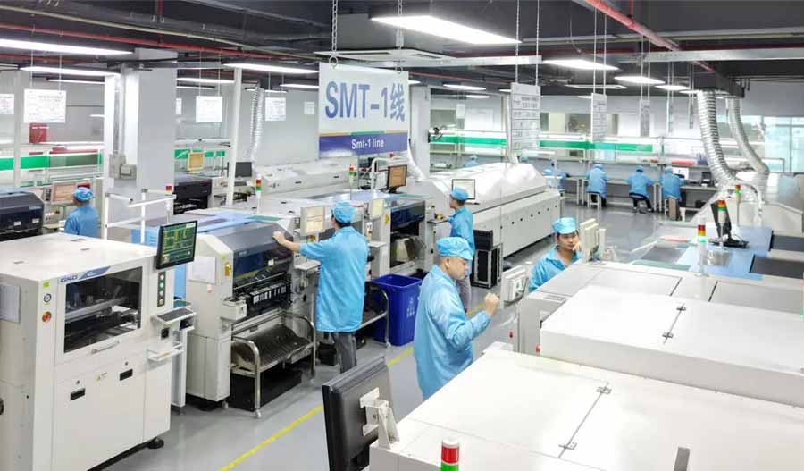
High-Complexity PCBA Assembly Engineering Capability of EMS Providers
A major issue we encounter with EMS (Electronic Manufacturing Services) providers is the lack of tiered classification among them. There is no clear benchmark to determine their suitability for high-complexity boards based on personnel competency, equipment capability, and on-site process control. We have considered different approaches for different suppliers, such as designating specific production lines. However, questions remain: Does this approach contribute to the overall capability improvement of the EMS provider? Are there clear requirements for enhancing personnel skills? Furthermore, quantifying the capability of a designated line is problematic. For example, the specific correlation between personnel technical skills and equipment capabilities required for a board with a complexity score above 200 is not clearly defined.
Assembly Requirements for High-Complexity PCBA
Whether for EMS providers offering assembly services or for in-house processing, the control of high-complexity PCBA can be quantified into five aspects: Man, Machine, Material, Method, and Environment.
- Man: Designate dedicated production lines for processing high-complexity boards. Establish strict regulations and requirements for equipment maintenance and operators, including training, testing, and qualification standards.
- Machine: Implement strict control requirements for every piece of equipment on each high-complexity product line, including detailed operating instructions and inspection protocols.
- Material: Control and reduce tube-packaged components. Ensure dimensional stability and solder terminal consistency for miniature components like 0402 and 0201. Check PCBs for significant warpage. Ensure that the solder temperature requirements for various component plating/finishes and solder terminals are largely consistent. Ensure that the deformation of large connectors and module packages during reflow soldering remains within allowable limits.
- Method: For process procedure control, we currently have a control specification exceeding 30 pages for high-complexity PCBA assembly. Every step is strictly controlled, from pre-loading the board, solder paste printing, paste replenishment and changeover, to pre-use stencil inspection, and even the wipes and cleaning solvents used.
- Environment: Implement strict controls across all aspects: material storage conditions, ESD (Electrostatic Discharge) management, moisture-sensitive device management, and the storage and handling of IC components.
Application Value of the PCB and PCBA Complexity Quantification Method
EMS providers can adopt different strategies in personnel composition, equipment configuration, and process control for PCBA of varying complexity levels, forming tiered manufacturing capabilities to meet diverse customer needs. Different processing fees can be justified based on different PCBA complexity levels.
Through the implementation of practices for high-complexity PCB and PCBA, ODM (Original Design Manufacturer) companies have seen significant improvements in PCB fabrication yield and PCBA assembly quality. This has reduced rework costs and reliability risks, yielding substantial economic benefits. The method can also be used to assess personnel allocation, process design strategies, and management model optimization.
Currently, PCB and PCBA quantification standards are applied by a few companies but have not gained widespread recognition and adoption across the industry. Furthermore, the parameters involved in these quantification standards are not yet comprehensive and require further optimization. It necessitates the participation of industry peers to develop unified PCB and PCBA quantification standards and promote their implementation within the sector.