


Case Background
A camera module, in the process of production testing of dysfunctional failure, after a preliminary analysis, the judgement may be the LGA package main chip abnormality.
Analysis process
X-ray analysis


Test results: No obvious abnormality was found in the LGA welding of the two failed samples.
Staining Analysis
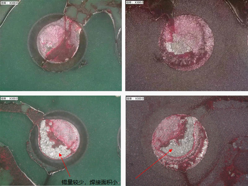
Test results: Sample 1 will be LGA staining test after stripping, found that most of the solder joints have a small amount of tin phenomenon, welding area is small; a small number of presentations for the combination of no solder, it can be confirmed as a bad virtual welding.
Cross-sectional analysis

Test results: Sample 2 was analysed in cross-section, and the LGA was found to be poorly soldered in many places, with a small amount of tin in the solder pads, showing a phenomenon of false soldering.
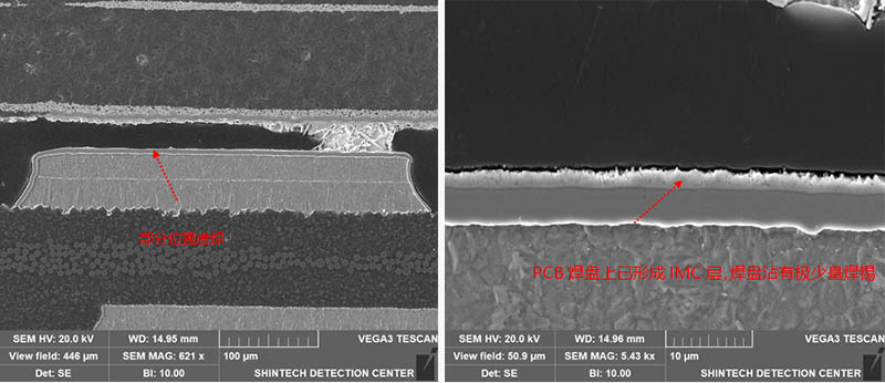
SEM Analysis
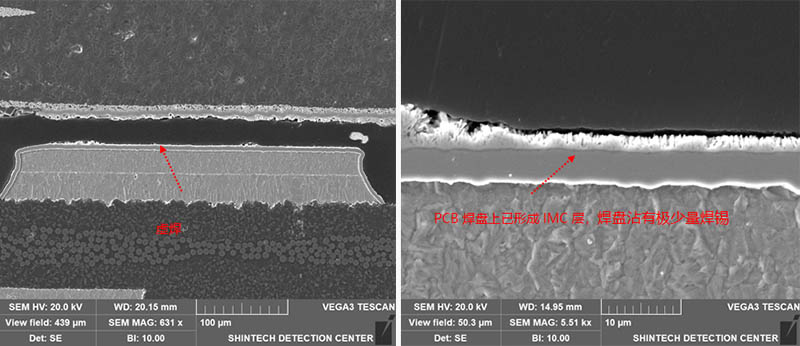
Test results: SEM analysis of the failed solder joints, PCB pads have formed IMC layer, the pads are stained with a very small amount of solder, the device pads are not attached to the solder.
Test Result: There is obvious tin less.
EDS Analysis

Test result: EDS analysis of the virtual solder joints, no obvious abnormal elements.
Analysis results
Through staining test, cross-section analysis and SEM analysis, EDS analysis determined that the main causes of LGA soldering failure are – insufficient amount of solder paste leads to the bottom of the soldering solder.
Improvement programme
1.Printing stencil opening design and printing process parameters to improve;
2.LGA chip mounting pressure verification.