


In an electronics manufacturing company producing complex devices with multiple integrated circuit (IC) chips, a recurring issue has been identified on some circuit boards: IC lead floating and non-wet solder, commonly referred to as “floated soldering” or “IC lead floating and non-wet” . This defect significantly threatens product performance, stability, and reliability. Ensuring consistent and reliable solder joint quality is paramount in electronics manufacturing to prevent such issues.
What is IC Lead Floating and Non-Wet Solder?
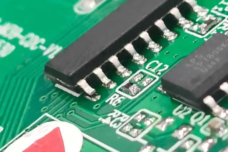
This defect occurs when the leads (pins) of an Integrated Circuit do not form a proper metallurgical bond with the corresponding pads on the Printed Circuit Board (PCB). Visually, the lead may appear to be sitting above the solder joint or not wetted by solder, resulting in an incomplete or weak connection . In surface mount technology (SMT), this is often associated with issues like insufficient solder, poor wetting, or “pillow effect” where the solder paste melts but fails to coalesce with the component lead .
Impacts of IC Lead Floating and Non-Wet Solder
The consequences of this defect are severe and multifaceted:
- Unreliable Electrical Connection: The primary function of a solder joint is to provide a continuous electrical path. A non-wet or floated lead creates an intermittent or open circuit . This leads to unpredictable current flow, signal transmission failures, and complete loss of functionality in the affected circuit section .
- Signal Degradation and Increased Noise: Poor electrical connections act as sources of impedance and can introduce signal distortion and electrical noise . This degrades signal integrity, leading to erratic circuit behavior, data errors, and reduced operational stability.
- Thermal Management Issues: Solder joints are crucial for heat dissipation from components to the PCB. A floated lead creates a point of high thermal resistance, causing heat to concentrate . In high-power or high-temperature applications, this can lead to localized overheating, accelerated aging of the component, and premature failure.
- Compromised Mechanical Strength: Solder provides the mechanical bond that anchors the component to the board. A non-wet joint lacks this strength, making the IC susceptible to vibration-induced failure, lead breakage, or complete detachment from the PCB during handling or operation .
- Reduced Product Reliability and Lifespan: If not detected during production, these latent defects lead to field failures, increased warranty costs, and a significant reduction in the end product’s overall reliability and operational lifespan .
Root Causes of IC Lead Floating and Non-Wet Solder
The defect stems from a combination of factors in materials, process, and design:
- Solder Paste/Insufficient Solder: The most direct cause is an inadequate amount of solder paste deposited on the pad . This can be due to stencil aperture issues (too small or clogged), low stencil pressure, or poor paste transfer efficiency.
- Oxidation and Contamination: The solderability of both the component lead and the PCB pad is critical. Oxidation layers, organic contamination, or moisture on these surfaces prevent the molten solder from wetting and spreading properly . This is a common cause of poor wetting.
- PCB and Pad Design Flaws: Poor design is a major contributor. Examples include pads connected to large ground planes (acting as heat sinks that cool the pad too quickly), unbalanced pad geometries for two-terminal components (leading to tombstoning), or the presence of via-in-pad without proper filling, which can siphon solder away from the joint .
- Reflow Soldering Process Issues: An improper temperature profile during reflow can cause defects. Insufficient peak temperature or time above liquidus (TAL) results in “cold solder,” where the paste does not fully melt and coalesce . Conversely, excessive temperature can cause solder balling or oxidation. Uneven heating across a component’s leads can create tension that pulls one lead up, causing floating.
- Component and Placement Problems: Warped or coplanarity issues with IC leads, misalignment during placement where the lead is not centered on the pad, or the use of components with poor solderability can all lead to non-wet joints .
Comprehensive Solutions and Preventive Measures
A systematic approach across design, materials, and process control is required to solve and prevent this issue.
Optimize Stencil Design and Solder Paste Printing:
- Review and modify the stencil aperture design. For critical components like QFNs or BGAs, slightly increasing the aperture size or using a stepped stencil to deposit more paste can be effective . Ensure the aperture area ratio meets IPC guidelines to guarantee good paste release.
- Strictly control the solder paste printing process. Regularly maintain stencils and squeegees, verify printing alignment, and monitor paste volume using SPI (Solder Paste Inspection) systems.
Ensure Surface Solderability and Implement Proper Storage:
Enforce strict controls on component and PCB storage to prevent oxidation. Use moisture-sensitive device (MSD) protocols, including baking components before use if indicated by humidity indicator cards .
Incoming inspection should verify the solderability of leads and pads. For known oxidation issues, consider using a more active flux formula within the solder paste, though this must be balanced with post-solder cleanliness requirements .
Refine the Reflow Soldering Profile:
Develop and validate a robust reflow temperature profile. Ensure the profile provides adequate preheat to activate the flux and remove volatiles, followed by sufficient time above the solder’s liquidus temperature (e.g., 40-100 seconds above 217°C for SAC305) to ensure complete melting and wetting .
For components with large thermal mass differences, use a profile with a longer soak zone to equalize temperature across the board and prevent component-specific cold soldering.
Review and Improve PCB Design:
Collaborate with the design team on Design for Manufacturability (DFM). Use thermal relief connections for pads attached to large copper pours to slow down heat dissipation during soldering .
Avoid via-in-pad designs for standard processes. If necessary, specify that vias must be filled and planarized.
Ensure pad sizes and geometries are symmetrical for passive components to prevent tombstoning.
Enhance Process Control and Inspection:
Implement Automated Optical Inspection (AOI) after reflow to visually detect placement misalignment, floating components, or obvious non-wet joints .
For critical assemblies with BGAs or QFNs, employ X-ray inspection to reveal hidden solder joint defects like voids, bridging, or non-wet underneath the component .
Consider destructive analysis techniques like the “Red Dye Penetration Test” for failure analysis to conclusively identify the location and extent of non-wetting in field returns or for process validation .
Staff Training and Procedure Adherence:
Ensure all operators and process engineers are thoroughly trained on the causes and impacts of soldering defects. Emphasize strict adherence to Standard Operating Procedures (SOPs) for material handling, machine operation, and inspection .
By addressing the root causes through this multi-faceted strategy—encompassing design optimization, material control, process precision, and rigorous inspection—electronic manufacturers can effectively eliminate IC lead floating and non-wet solder defects, thereby significantly enhancing product yield, reliability, and customer satisfaction.