


Modern electronic products utilize high-power components such as high-performance processors, MOSFETs, high-power LEDs, and IGBTs. As the electronics industry evolves, these components continue to shrink in size, which often leads to increased heat generation. Elevated temperatures can readily cause device failures, making thermal management in PCBs essential.
This article introduces 14 PCB thermal management techniques to mitigate heat buildup in printed circuit boards.
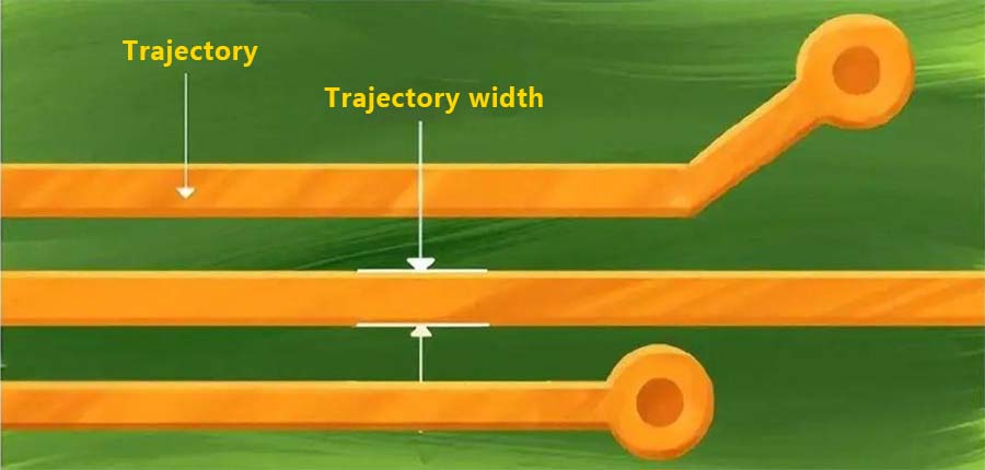
1、Identifying Hotspots and High-Current Traces
To achieve thermally stable PCBA, thermal effects must be analyzed during the design phase. The initial step in thermal design is hotspot identification through thermal modeling or simulation techniques. Additionally, current analysis is crucial since high-current traces contribute significantly to heat generation.
1.1. Proper geometric arrangement of components and high-current traces promotes even heat distribution.
1.2. High-current traces must be kept away from thermally sensitive components such as sensors and operational amplifiers.
2、Copper Thickness and Trace Width
The thickness and width of copper pads or traces play a vital role in PCB thermal design. Copper traces should be sufficiently thick to provide a low-impedance path for the current. The resistance of copper traces and vias results in notable power loss and heating, particularly under high current density. Thus, adequate trace width and thickness are recommended to minimize heat generation.
3、Pad Design
Similar to trace thickness, pad thickness is critical as heat dissipates directly through the top copper layer. Therefore, top copper pads must have sufficient thickness and area to enable adequate heat dissipation.
3.1. If heat sinks are incorporated into the PCB design, they are typically mounted on bottom copper pads. These pads should offer sufficient coverage to optimize heat transfer to the heat sink.
3.2. Component pins are soldered to and supported by pads, creating a direct connection that results in very low thermal resistance. Thermal relief pads—special pads connected to the surrounding copper via thin bridges—are often used.
3.3. Solder used to connect component footprints to thermal pads should be minimized. Excessive solder under thermal pads can cause components to float on molten solder during reflow, leading to unwanted movement. Optimizing solder volume addresses this issue.
4、Placement of High-Power Components on PCB
For improved thermal performance, high-power components such as processors and microcontrollers should be positioned near the center of the PCB. Placement near the edge can cause heat accumulation and elevated local temperatures. In contrast, central placement allows heat to dissipate in all directions across the board surface, resulting in lower surface temperatures and more efficient dissipation.
Additionally, high-power components should be placed away from sensitive devices, and adequate spacing should be maintained between multiple high-power components. Even distribution across the PCB is advised.
5、Thermal Vias for Heat Dissipation in PCBs
Thermal vias offer a straightforward method for board-level cooling. Understanding thermal resistance is key: it quantifies the opposition to heat flow through a conductor, defined as the temperature difference across two points divided by the total heat flow (R = ΔT / P, where R is thermal resistance in °C/W or K/W, ΔT is the temperature difference in °C, and P is power in W).
Higher resistance impedes heat flow and dissipation. Thicker materials exhibit lower resistance, so PCBs with thicker, low-resistance materials dissipate heat more effectively.
Thermal vias—conductive metal barrels—provide a low-thermal-resistance path from the top copper to the bottom surface. Placed directly beneath heating components, they facilitate dissipation via conduction.
5.1. Thermal Via Structure
While no perfect design exists, a general thermal via structure includes:
5.1.1. Enhanced copper thickness in the via contact.
5.1.2. Vias filled with conductive epoxy and capped with copper, acting as heat pipes to transfer heat away from hotspots.
5.1.3. Sealing with solder mask to ensure reliable soldering of connected components.
5.2. Placement of Thermal Vias in the Board
Strategic placement and arrangement of thermal vias, which have higher thermal conductivity than FR4, are critical.
Each via possesses inductance. Interestingly, parallel vias connected to a ground plane provide the lowest inductance return path if the bottom conductor of the heating component is grounded. Maximizing the number of thermal vias reduces thermal resistance and accelerates heat transfer.
The number of vias under power ICs and processors should be determined based on thermal budget and surface area. Increasing via length or width can compensate for budget constraints.
5.2.1. Limitation: Thermal vias primarily enhance local dissipation; their impact is confined to specific regions.
5.2.2. Benefit: Compliance with IPC-2152 standards for thermal performance.
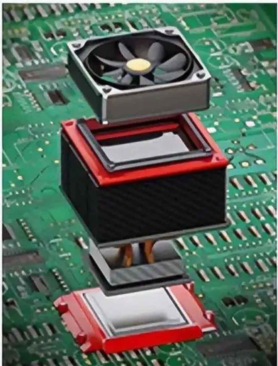
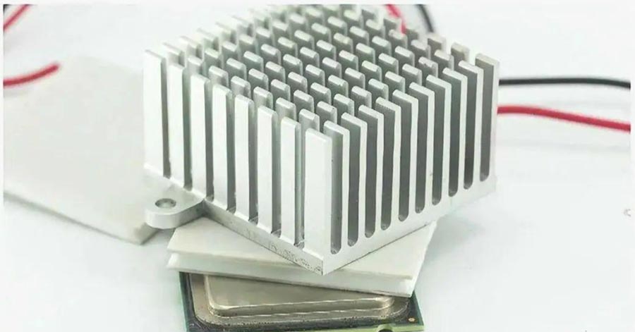
6、Heat Sinks
Heat sinks transfer heat from PCB components to a cooling medium via conduction—moving heat from high to low thermal resistance areas, proportional to the temperature difference. Heat sinks absorb PCB heat and provide extended surface area for faster dissipation.
Selection depends on factors such as the thermal resistivity of materials, coolant velocity, thermal interface materials, fin count and spacing, and mounting techniques.
7、Integrated Heat Pipes
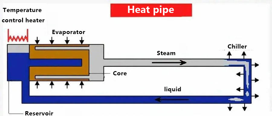
Heat pipes are cooling devices recommended for high-temperature applications like rockets, satellites, and avionics. Typically hollow cylinders, they can be custom-shaped.
Heat from devices vaporizes liquid within the pipe. The vapor condenses at the condenser end and returns to the evaporator via capillary action through a wick structure, ensuring continuous heat removal.
Heat pipes should fully cover heat sources and allow bending per design requirements. Working fluids range from refrigerants to liquid metals, selected based on temperature range and chemical compatibility with the container and wick.
8、Thicker PCB Boards
For compact devices, cooling methods like heat sinks, heat pipes, or fans may not be feasible. Increasing board thermal conductivity and dispersing heat become the only options. Thicker boards with larger surface areas dissipate heat more rapidly.
Thermal conductivity depends on the coefficient of thermal expansion (CTE) and thickness of materials used. Careful material selection for each layer is essential; CTE mismatch between layers can reduce thermal conductivity under repeated thermal cycles. Plated copper in vias and solder balls is particularly vulnerable under high thermal cycling.
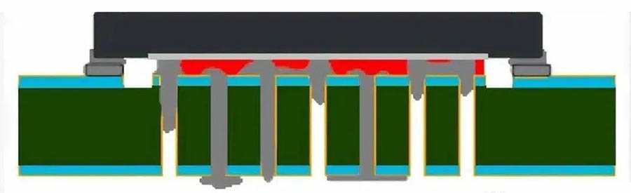
9、Integrated Cooling Methods
Integrated cooling methods achieve higher thermal conductivity compared to traditional heat sink and fan setups. This approach involves blowing coolant directly onto the bottom of processors, BGAs, or other heating components through dedicated vias.
The number of vias should be determined by the thermal requirements of mounted components. Start with a single via and add more based on coolant velocity and component surface area.
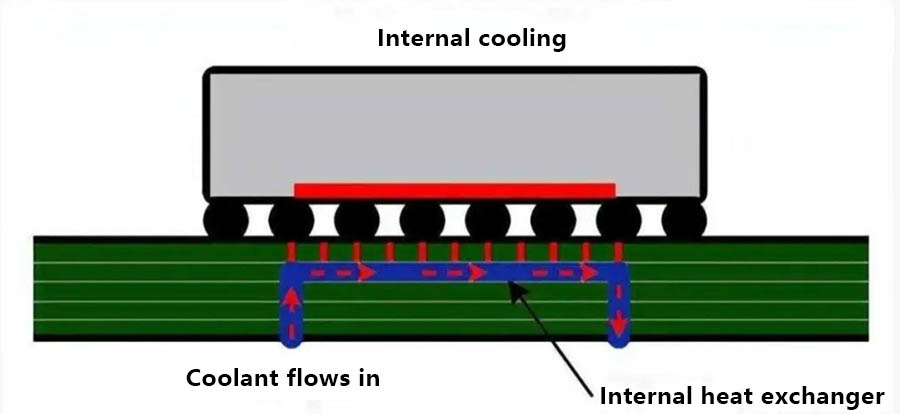
Other integrated cooling methods include internal heat exchangers, as illustrated above. Here, a heat exchanger is embedded within the board, eliminating the need for external heat sinks or cold plates, thus reducing assembly steps and product weight. However, these coolers require very high thermal via density around cooling channels.
10、Cooling Fans
While previous methods rely on conduction, which may be insufficient in many cases, cooling fans employ convective heat transfer, offering highly effective heat removal from components.
Fan efficiency depends on the ability to expel a specific volume of air and compatible placement. Factors like friction, size, noise, cost, operation, and power requirements must be considered, but airflow capacity remains the superior factor in selection.
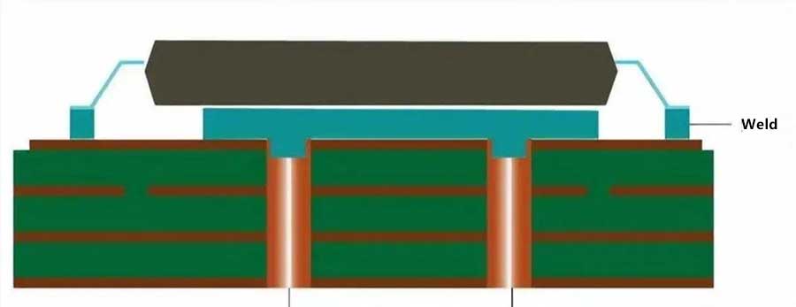
11、Solder Concentration
Solder thickness at device joints should be uniform and environmentally stable to reduce heat buildup at component leads. Extra care is needed near vias to prevent overfilling, which can cause bumps on the board bottom and reduce heat sink contact area.
Two methods to avoid solder overflow:
11.1. Reduce via diameter to below 0.3 mm. Smaller vias allow surface tension of molten solder to better resist gravity.
11.2. Tent vias by covering pads with solder mask to prevent solder flow through.
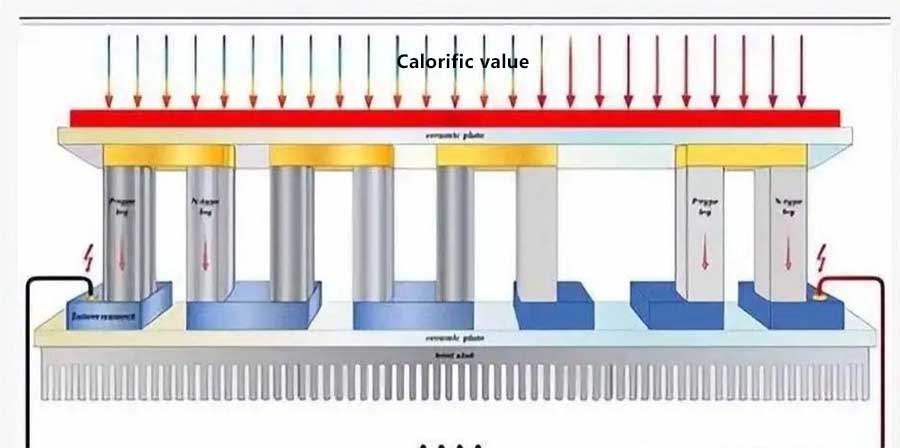
12、Peltier Heat Pumps / Thermoelectric Coolers
This advanced cooling technology uses the Peltier effect for cooling, which can reduce component temperatures below ambient levels—opposite to heat generation.
TECs are used where precise temperature control is required, such as in CCD cameras, laser diodes, microprocessors, and night vision systems. They offer accurate temperature control and fast response.
TECs can be combined with air or liquid cooling to extend the limits of traditional cooling for high-power processors. Commercial Peltier pumps range in size from 3.2×3.2 mm² to 62×62 mm² on the cooling side and 3.8×3.8 mm² to 62×62 mm² on the base (heating side).
13、Thermal Interface Materials (TIM)
Thermal Interface Materials (TIM) are used between heat-generating and heat-dissipating components to reduce contact thermal resistance. They play a critical role in thermal management.
Microscopic gaps between microelectronic surfaces and heat sinks reduce actual contact area to about 10% of the heat sink base area, with the rest being air gaps. Since air has low thermal conductivity (0.024 W/(m·K)), contact thermal resistance is high, hindering heat conduction and reducing散热器 efficacy. TIMs fill these gaps with high-thermal-conductivity materials, eliminating air and establishing efficient heat transfer channels, significantly reducing thermal resistance.
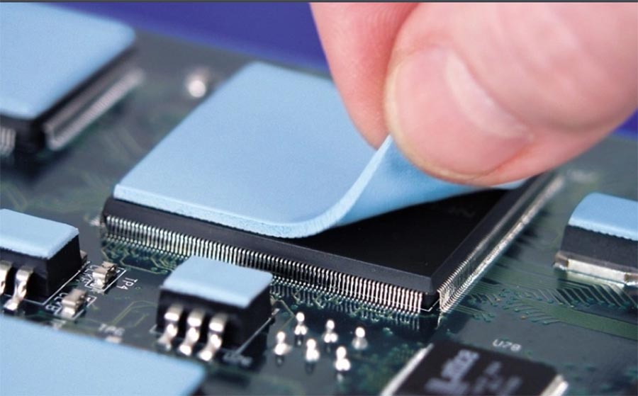
TIMs include:
– Thermal grease
– Thermal gel
– Thermal pad
– Phase change material
– Phase change metal alloy
– Thermal conductive adhesive
Detailed characteristics are provided in the table.
|
Materials
|
Typical components
|
Advantages
|
Disadvantages
|
Thickness
(mil)
|
Thermal conductivity
(W/m.K)
|
|---|---|---|---|---|---|
|
Thermal grease
|
Silicone oil base, ZnO, Ag, AlNl
|
High thermal conductivity, adheres readily to surfaces, requires no curing, and is reusable.
|
There is a pumping-out effect and phase separation, mobility, and it becomes dirtier during production.
|
2
|
3-5
|
|
Thermal gel
|
Al, Ag, silicone oil, olefin, paraffin
|
High thermal conductivity, adheres readily to surfaces prior to curing, exhibits no pumping effect or migration, and is reusable.
|
It needs to be solidified and its thermal conductivity is lower than that of silicone grease.
|
1-1.5
|
3-4
|
|
Phase change material
|
Polyolefin resin, acrylic resin, aluminium, aluminium oxide, carbon nanotubes
|
Adheres readily to surfaces without curing, exhibits no delamination, is easy to apply, and is reusable.
|
The thermal conductivity is lower than that of silicone grease, and the thickness is uneven.
|
1.5-2
|
0.5-5
|
|
Phase change metal alloy
|
Pure indium foil, indium/silver, tin/silver/copper, indium/tin/bismuth
|
High thermal conductivity, easy to use, reusable
|
May dissolve completely, leaving cavities.
|
2.0-5
|
30-50
|
|
Thermal conductive adhensive
|
Epoxy resin substrate, iron, silver, nickel
|
High thermal conductivity, requiring no normal pressure
|
It needs to be solidified. During the solidification process, a fixture is required. The thermal conductivity is lower than that of silicone grease and there is a possibility of detachment.
|
N/A
|
N/A
|
|
Thermal pad
|
Silicone rubber, fibreglass, polyester substrate, silicone oil-filled
|
Easy to use, reusable, flexible and adaptable
|
Lower thermal conductivity than thermal grease, with a thicker and more uneven layer.
|
10-100
|
1.5-4
|
14、Thermal Simulation of PCBs
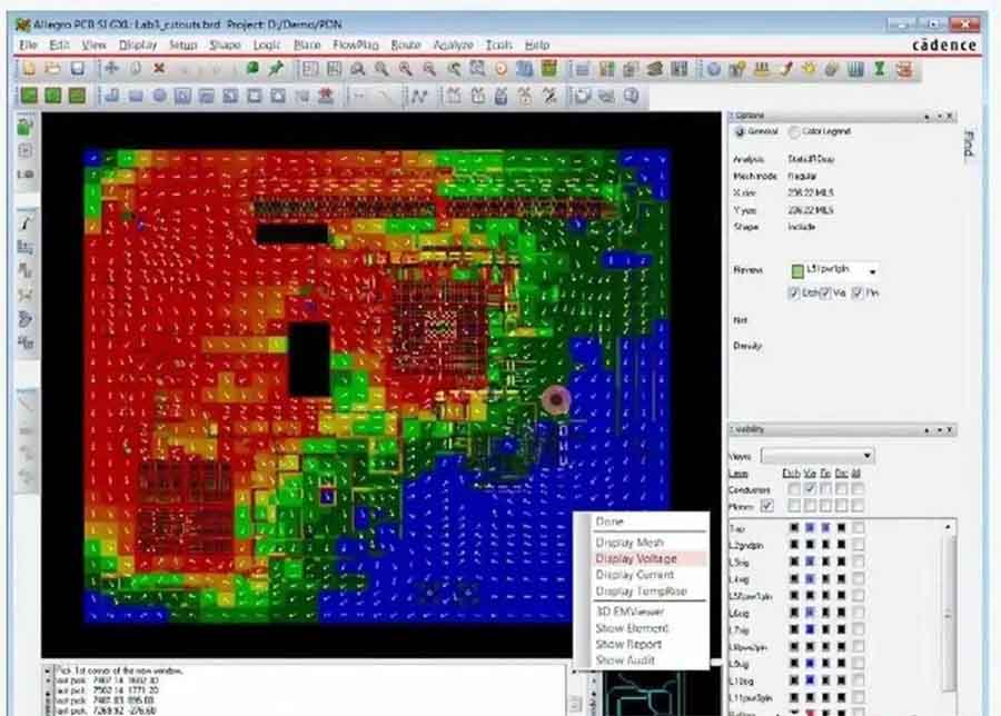
Detailed thermal simulation helps precisely locate temperature hotspots on PCBs. Thermal simulations produce color-scale maps of temperature distribution under various conditions, with temperatures in Celsius (°C). These maps are generated by calculating temperatures at thousands of points on the PCB.
Why perform thermal simulation?
14.1. Locate hotspots to avoid device failure risks.
14.2. Assess reliability of dielectric materials with various CTE values to improve product reliability.
14.3. Reduce implementation costs by minimizing engineering delays, field failures, and product iterations.
14.4. Enhance performance and communication between engineering and electrical teams.
TORTAI: Your Expert in PCBA Thermal Management
TORTAI possesses extensive experience and expertise in PCBA thermal management. We provide professional advice during the DFM stage to optimize PCB stack-up, copper planes, and via design. Our manufacturing process strictly controls techniques to ensure the quality of thermal via filling and correct application of TIMs. We offer end-to-end PCBA solutions from design to manufacturing and testing for high-reliability industries such as medical, automotive, industrial control, and new energy, ensuring exceptional performance and long-term reliability under stringent conditions.
Choose TORTAI to ensure your innovative products overcome thermal challenges, operate stably, and succeed in the market.