


In the development of electronic products, EMC (Electromagnetic Compatibility) test failure is a rite of passage nearly every hardware engineer must face. Industry data shows that up to 50% of products fail their first EMC test, and the failure rate during trial production due to EMC design defects exceeds 35% . The cost of post-test remediation is typically 6–10 times higher than addressing EMC during the design phase . For power PCBA, the inherent switching nature of power conversion makes it the dominant source of electromagnetic interference (EMI) — switch-mode power supplies account for over 60% of electromagnetic disturbance issues in electronic equipment .
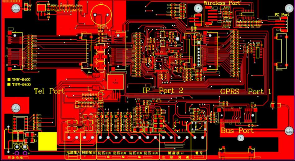
1. The Nature of EMC: The Three Elements of Interference
Every EMC problem consists of three essential elements: a source, a coupling path, and a victim. The core of EMC design is to break this chain .
1.1 Identifying the Interference Source
The primary source of interference in power PCBA is the high-speed switching of the power MOSFET. When the switch transitions from on to off, both current and voltage undergo abrupt changes, and the steep edges contain a broad spectrum of high-frequency harmonics.
- Switching node (SW node):Voltage slew rate (dv/dt) can reach 50 V/ns, generating intense electric field radiation.
- Reverse recovery of the freewheeling diode:Creates high-frequency current spikes, introducing common-mode noise.
- High-frequency current loop:The larger the loop area, the higher the current slew rate (di/dt), and the stronger the radiated emissions.
1.2 Coupling Paths
EMC interference propagates through two primary mechanisms:
- Conducted emissions:Travels through conductors such as power lines and signal cables, primarily in the 150 kHz to 30 MHz frequency range .
- Radiated emissions:Propagates through space as electromagnetic waves, dominant in the 30 MHz to 1 GHz range .
1.3 Sensitive Victims
Precision components such as ADCs, sensors, and MCUs are particularly susceptible to interference and require dedicated protection .
2. The Four Core Principles of EMC Design
Principle 1: Minimize Loop Area
The larger the high-frequency current loop area, the stronger the radiated emissions. Testing shows that for every 50% increase in loop area, switching noise rises by 6 dB . For a buck converter, the high-frequency loop includes “input capacitor → high-side MOSFET → low-side MOSFET → input capacitor.” The high-frequency ceramic capacitor (X7R dielectric) must be placed directly adjacent to the IC’s VIN and GND pins, avoiding vias that would add parasitic inductance.
Rule of thumb: The ideal loop area should be kept under 1 cm², and the power loop area should not exceed 5 cm² .
Principle 2: Functional Zoning
Partition the PCB by circuit function. Place noise sources (switch-mode power supply, power drivers) separately from sensitive circuits (analog, sensors, MCU), maintaining a spacing of ≥ 5 mm. Interference sources should be located near the PCB edge to allow radiated energy to dissipate away from internal circuitry.
Principle 3: Maintain a Continuous Reference Plane
Keep the ground plane and power plane intact and continuous to provide a low-impedance return path for signals. For multilayer boards, alternate signal layers with ground planes. A recommended stack-up for 4-layer boards is: Signal → Ground → Power → Signal .
Principle 4: Coordinate Filtering and Grounding
Place filtering components (X capacitors, Y capacitors, common-mode chokes) strategically to cut conducted interference paths. Optimize the grounding design to ensure that interference currents are quickly shunted to ground.
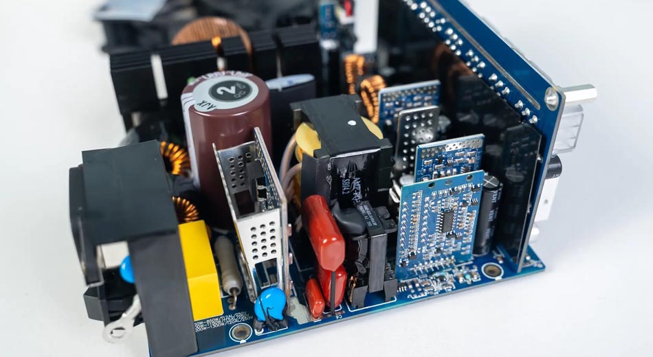
3. Practical Design Techniques: From Schematic to PCB Layout
3.1 Schematic Stage: Source Suppression
Filter Design
The input port is the first line of defense against conducted emissions. The recommended combination is common-mode choke + X capacitor + Y capacitor:
- Common-mode choke:Inductance of 1 mH to 10 mH; rated current should be at least 30% higher than the actual operating current to avoid saturation .
- X capacitor:Connected between line and neutral; typical value 1 μF to 1 μF (X2 safety-rated) .
- Y capacitor:Connected from line to ground and neutral to ground; typical value 10 nF to 100 nF (Y1 or Y2 safety-rated). Leakage current limits must be observed .
Snubber Circuit
An RC snubber connected across the drain and source of the switching MOSFET effectively reduces voltage ringing. Typical values: capacitor 100 pF to 1 nF, resistor tens to hundreds of ohms. Tune the values so that the voltage spike is reduced to an acceptable level.
Component Selection
Use synchronous rectification topologies and DC-DC converters with integrated MOSFETs to significantly reduce the high-frequency loop area. Where efficiency permits, configure the IC to operate in forced PWM mode (FPWM) to avoid frequency jittering at light loads, which can degrade EMC performance.
3.2 PCB Layout Stage: Key Implementation Steps
Power Loop Layout
For a buck converter, the high-frequency current loop includes the input capacitor, high-side MOSFET, and low-side MOSFET. The input capacitor must be placed directly adjacent to the IC’s VIN and GND pins, with trace lengths kept under 3 cm. The SW node (switching node) should not have large copper areas — test data shows that reducing the SW copper area by 30% lowered radiated noise at 30 MHz by 8 dB .
Grounding Design
Grounding is a common source of EMC design mistakes. Typical errors include:
- Randomly splitting the ground plane, forcing return currents to take long detours and forming large loops.
- Connecting digital and analog grounds at multiple points, creating ground loops that couple noise.
Correct approach: Partition the ground into digital ground (DGND), analog ground (AGND), and power ground (PGND). Connect each section with dedicated copper, and join them at a single point (using a 0 Ω resistor or ferrite bead) near the power input. Ground trace width should be ≥ 2 mm for 1 oz copper, and ≥ 3 mm for power ground .
Protecting Sensitive Signals
Feedback lines, compensation traces, and other small-signal routing should be kept away from power traces and high-frequency nodes, maintaining a spacing of ≥ 3× the trace width (3W rule) . Critical signals such as clock and reset lines can be protected with guard traces — copper pours on both sides, with ground vias placed at intervals of λ/20.
3.3 Shielding and Heatsink Treatment
When a heatsink is attached to a switching MOSFET, the parasitic capacitance between the heatsink and the MOSFET drain couples high-frequency noise to the heatsink, effectively turning it into an antenna. A practical solution: insert an insulated aluminum foil between the heatsink and the MOSFET, and ground the foil. This breaks the coupling path and reduces radiated emissions.

4. TORTAI Technologies Case Study: 24V/50A Industrial Power Supply EMC Retrofit
Problem: An industrial power supply module failed EMC testing with radiated emissions exceeding 68 dBμV/m in the 30–200 MHz band — 28 dB above the EN 55032 Class B limit (40 dBμV/m).
Root Cause Analysis:
- Power loop area was excessively large (32 mm²), creating a strong radiation source.
- SW node copper area was too large, acting as an antenna.
- Input filtering was insufficient; a common-mode choke was missing.
Corrective Actions Taken:
- Layout optimization:Power loop area reduced from 32 mm² to 9 mm²; SW node copper area minimized.
- Filtering upgrade:Added a π-filter at the input (10 μH inductor + 100 nF capacitor + 10 nF capacitor).
- Shielding:Installed a 8 mm thick aluminum shield over the high-interference region.
Result: Radiated emissions dropped to 41 dBμV/m, passing EN 55032 Class B. The overall retrofit cost was reduced by more than 60% compared to a full redesign.
5. Frequently Asked Questions (FAQ)
Q1: Where do EMC problems typically originate in power PCBA?
A: According to industry statistics, 80% of EMC issues stem from PCB layout design. The most common cause of radiated emission failure is an excessively large power loop area, followed by improper grounding that introduces common-mode interference. Optimizing the high-frequency loop during layout can save up to 80% of retrofit costs.
Q2: How should decoupling capacitors be placed for maximum effectiveness?
A: Placement is critical. The high-frequency ceramic capacitor (0.1 μF) must be placed directly next to the IC power pin, with a distance of ≤ 3 mm, a ground path of ≤ 3 mm, and no more than one via. Measurements show that moving the capacitor from 10 mm away to 3 mm away reduced power ripple from 150 mV to 20 mV and lowered conducted emissions by 12 dB.
Q3: How should a common-mode choke be selected and placed?
A: Selection: Inductance of 1 mH to 10 mH, rated current 30% above the actual operating current to prevent saturation. Placement: Position the choke vertically at the power input; do not place copper under the choke to avoid parasitic coupling. For the 150 kHz to 30 MHz range, a PQ3220 core (10 mH) paired with an X capacitor (0.1 μF) and Y capacitor (10 nF) is recommended .
Q4: Should the ground plane be split? How to do it correctly?
A: Ground plane splitting is a double-edged sword. For mixed-signal circuits, the recommended approach is functional zoning with a unified ground plane: physically separate digital and analog sections, but keep the ground plane continuous. Join the sections at a single point (0 Ω resistor or ferrite bead) near the power entry. If splitting is unavoidable, signal traces must never cross the split gap, as this forces return currents to take a long detour, dramatically increasing radiation.
Q5: How should the SW node (switching node) be handled?
A: The SW node experiences the most severe voltage transients (dv/dt up to 50 V/ns). Three key rules:
- Minimize copper area— keep SW copper area under 15 mm² to avoid antenna effects.
- Place a solid ground plane directly beneath the SW nodeto act as shielding.
- Keep sensitive signal traces at least 3× the PCB layer spacing awayfrom the SW node.
- In multilayer boards, a ferrite bead (100 Ω @ 100 MHz)can be added in series with the SW node path to absorb high-frequency ringing.

Conclusion
EMC design for power PCBA is not a post-test repair task — it is a systematic engineering discipline that begins with topology selection, extends through schematic design, and culminates in PCB layout. Mastering the three principles of source suppression, path blocking, and victim protection, together with the four core rules of loop minimization, functional zoning, continuous reference plane, and coordinated filtering/grounding, will ensure first-pass success in the EMC lab and eliminate the pain of repeated board spins.
At TORTAI Technologies, we integrate EMC design review into our standard DFM (Design for Manufacturing) process. Backed by certifications including IATF 16949 and ISO 13485, we provide end-to-end EMC assurance from design pre-audit through volume production. EMC compliance is not the finish line — it is the foundation of product reliability.