


In high-speed PCBA design, the precision of trace width and spacing directly dictates the quality of impedance control. According to 2026 industry data from the electronics assembly manufacturing sector, 65% of circuit board failures originate from design defects, with 23% of customer designs incorporating extreme traces below 0.1 mm. This leads to impedance errors exceeding ±15% and a 3.8× increase in failure rates.
As a specialized provider in the high-reliability PCBA field for over a decade, TORTAI Technologies leverages its 4,600 m² modern facility in Humen, Dongguan, 4 fully automated high-speed SMT lines, and IATF 16949 certification. Through a “standard compliance + tolerance control” methodology in trace design, we have enabled over 50 clients to achieve mass production with zero impedance failures.
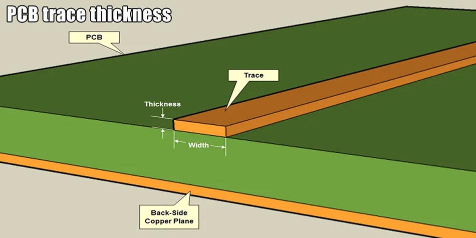
I. The Quantitative Basis: Why Violating Trace Width/Spacing Standards Guarantees Impedance Mismatch
1. Core Variable Relationships in the Characteristic Impedance Formula
According to IPC-2221 and the standard microstrip impedance model, the single-ended characteristic impedance formula is:

Where:
- Z₀ = Characteristic Impedance (Ω)
- εr = Dielectric Constant (FR-4 typical value: 4.2–4.5)
- H = Dielectric Thickness (mm)
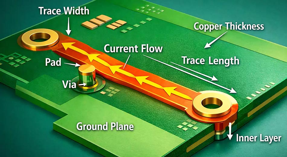
- W = Trace Width (mm)
- T = Copper Thickness (mm)
TORTAI Technologies Validation Data:
Using Rogers RO4350B substrate (εr = 3.66), 1/2 oz copper, and a dielectric thickness of 0.1 mm, the theoretical line width for a 50 Ω microstrip is 0.208 mm (8.2 mil).
| Trace Width Change | Impedance Impact |
|---|---|
| Decreased to 0.19 mm (7.5 mil, –8.5%) | Impedance rises to 54.3 Ω (+8.6%) |
| Increased to 0.226 mm (8.9 mil, +8.6%) | Impedance drops to 46.1 Ω (–7.8%) |
Differential Impedance Formula:

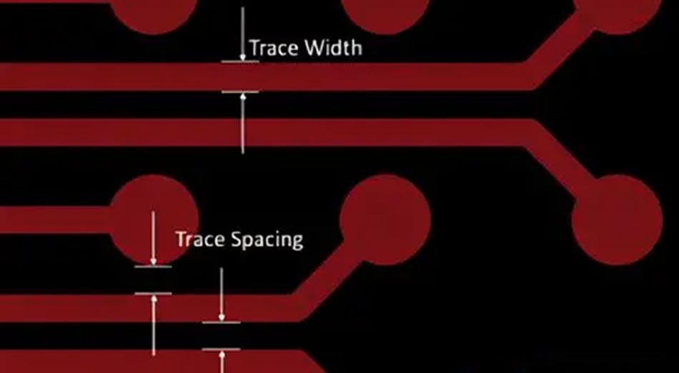
Where k is the coupling coefficient between traces. The smaller the trace spacing (S), the larger the coupling coefficient k. When the trace spacing S is less than 1.2× the trace width W, crosstalk attenuation degrades from –38 dB to –25 dB, causing impedance deviation to exceed ±10%.
2. The Amplifying Effect of Manufacturing Tolerances
Standard FR-4 multilayer board etching tolerances are ±10% (or ±25 μm), while high-precision HDI boards can achieve ±15 μm. The table below illustrates how trace width directly impacts impedance stability and yield:
| Trace Width | Etching Tolerance | Impedance Deviation | Mass Production Yield (FPY) |
|---|---|---|---|
| 0.15 mm (6 mil) | ±0.02 mm | +12% / –10% | 92% |
| 0.20 mm (8 mil) | ±0.015 mm | +8% / –7% | 98.7% |
| 0.30 mm (12 mil) | ±0.01 mm | +5% / –4% | 99.5% |
TORTAI Technologies utilizes a Laser Direct Imaging (LDI) process to control etching precision for 0.2 mm traces within ±0.01 mm. This stabilizes impedance deviation within ±7% and ensures a mass production first-pass yield (FPY) of ≥98.7%.
3. Industry Threshold Standards for Impedance Control
| Application Scenario | IPC Class | Allowed Impedance Deviation | Min. Trace Width / Spacing |
|---|---|---|---|
| Consumer Electronics | Class 1 | ±10% | 0.15 mm / 0.15 mm |
| Industrial Control | Class 2 | ±7% | 0.20 mm / 0.20 mm |
| Automotive Electronics | Class 2+ | ±5% | 0.25 mm / 0.25 mm |
| Medical / RF | Class 3 | ±3% | 0.25 mm / 0.20 mm |
Industry-grade PCBA requires trace width/spacing ≥ 0.2 mm as a baseline to keep impedance deviation within ±7%, preventing signal reflection and eye diagram closure.
II. TORTAI Technologies Impedance Failure Case Study
Project Background: Servo Drive PCBA
- Signal Type: CANopen differential signal (target impedance 100 Ω), 24 V control power supply
- Original Design Issue: Trace width 0.15 mm, spacing 0.15 mm → measured impedance 108 Ω (+8%). After 100 thermal cycles (–40 °C to +85 °C), communication Bit Error Rate (BER) reached 10⁻⁴
- Target Compliance: IPC Class 2 standard, impedance deviation ≤ ±7%, mass production FPY ≥ 98%
Optimization Solution
| Design Area | Original Design | TORTAI Optimized Design | Rationale |
|---|---|---|---|
| CANopen Differential Pair | 0.15 mm / 0.15 mm | 0.20 mm / 0.60 mm (3W Rule) | Spacing ≥ 3× trace width suppresses crosstalk |
| 24 V Control Loop | 0.15 mm / 0.15 mm | 0.20 mm / 0.20 mm | IPC Class 2 industrial standard |
| Power / Ground Plane | 0.15 mm / 0.15 mm | 0.30 mm / 0.30 mm | Reduces ground impedance, improves noise immunity |
Measured Results
| Metric | Original Design | Optimized Design | Improvement |
|---|---|---|---|
| Differential Impedance | 108 Ω (+8%) | 98 Ω (–2%) | Deviation reduced from +8% to –2% |
| Crosstalk Attenuation | –25 dB | –42 dB | +17 dB improvement |
| Temp. Cycle BER | 10⁻⁴ | 10⁻⁹ | –99.99% reduction |
| First-Pass Yield (FPY) | 72% | 98.7% | +26.7% |
III. PCBA Trace Width/Spacing Design Compliance Framework
All industrial and automotive-grade PCBA designs must comply with the following standards:
- IPC-2221 — Generic Standard on Printed Board Design
- IPC-2152 — Standard for Determining Current-Carrying Capacity in Printed Board Design (Thermal Management)
- IPC-A-610J Class III — Acceptability of Electronic Assemblies
- IEC 61076-2-101 — Connectors for electronic equipment (Industrial)
- GB/T 12668 — Adjustable speed electrical power drive systems (General Specification)
- IATF 16949:2016 — Automotive Quality Management System
IV. Frequently Asked Questions (FAQ)
Q1: Do all PCBA designs strictly require controlled trace width/spacing?
A: Low-speed, low-frequency circuits (e.g., LED drivers, simple control logic) can be relaxed to 0.15 mm. However, high-speed signals (>1 Gbps), differential transmission, and industrial/automotive-grade products must use ≥ 0.2 mm. Failure to do so increases the risk of impedance mismatch by 3.8×.
Q2: Can a 0.02 mm deviation in trace width destroy impedance control?
A: Yes. A 0.02 mm deviation on a 0.2 mm target (–10%) will cause impedance to rise by 8.6%, exceeding the IPC Class 2 threshold of ±7%.
Q3: What is TORTAI Technologies’ process capability for 0.2 mm traces?
A: Using LDI laser imaging, our tolerance is ±0.01 mm, impedance deviation ≤ ±7%, and mass production FPY ≥ 98.7%, fully compliant with IPC Class 2.
Q4: Why should differential pair spacing be at least 3× the trace width?
A: This is the 3W Rule. A spacing of ≥ 3× the trace width improves crosstalk attenuation from –25 dB to –42 dB, keeping differential impedance stable within ±5%.
Q5: Does the solder mask affect impedance?
A: Yes. The solder mask raises the effective dielectric constant, reducing impedance by 2 to 5 Ω. This must be accounted for in the design simulation.
Q6: Can TORTAI Technologies provide impedance test reports?
A: Yes. Every production batch ships with a full-board TDR (Time Domain Reflectometry) scanning report, making impedance deviation traceable to the specific production lot.
Q7: Does copper thickness variation cause impedance mismatch?
A: Yes. A ±10% fluctuation in copper thickness results in a ±3% impedance deviation. Designs must consider the “nominal thickness + tolerance” scenario when calculating worst‑case impedance.
Conclusion
Violating trace width and spacing standards inevitably leads to uncontrolled impedance. This is not a question of “probability,” but a deterministic outcome dictated by the laws of electromagnetics.
In the discipline of PCBA impedance control, TORTAI Technologies has specialized in high-reliability PCBA/OEM/ODM/EMS for over a decade. We are equipped with a 4,600 m² modern workshop, 4 fully automated high-speed SMT lines, 2 DIP insertion lines, and ICT/FCT testing lines. Our certifications include ISO 9001:2015, ISO 13485, and IATF 16949. We strictly adhere to IPC-A-610J Class III standards and operate a full MES traceability system.
Leveraging our accumulated expertise in IPC standard compliance (Class 2/3), impedance formula calculation (Z₀ deviation ≤ ±7%), LDI process control (0.2 mm trace width tolerance ±0.01 mm), and industrial compliance (IATF 16949 / GB/T 12668), TORTAI Technologies assists clients in early-stage design reviews of trace width and spacing. We provide a full lifecycle service from rule compliance to volume production verification, helping clients reduce the risk of impedance failures to zero and achieve mass production FPY exceeding 98%.