


In PCB design, the 6-layer board has become the mainstream choice for industrial control, automotive, and communications equipment due to its ideal balance of performance and cost.
Among these, the Top-GND-Signal-Power-Signal-Bottom stackup is one of the most classic and widely adopted structures. This article delves into the application scenarios, design essentials, and case studies of this stackup, combining IPC standards with the PCBA manufacturing experience of TORTAI Technologies.
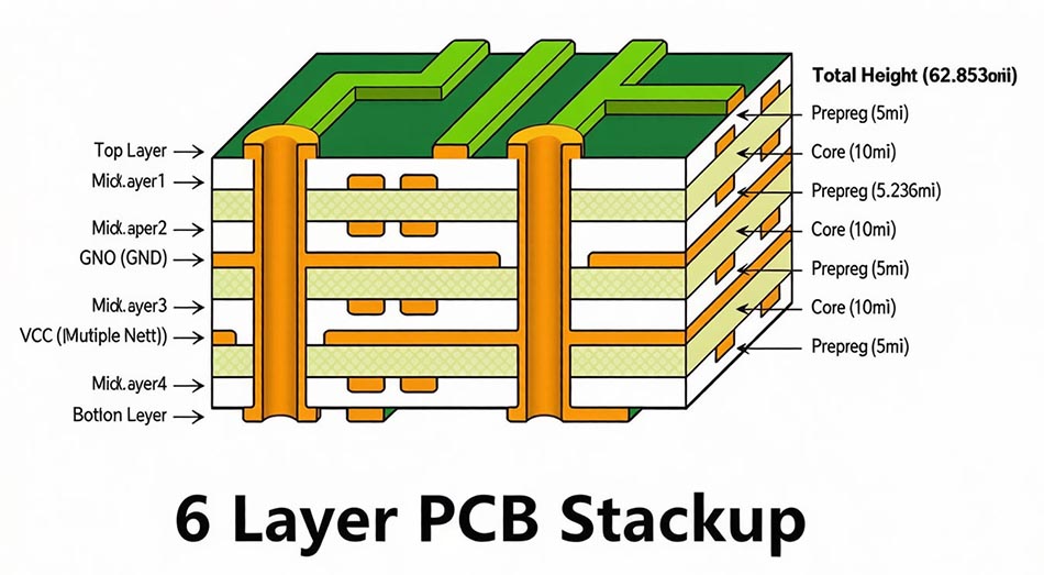
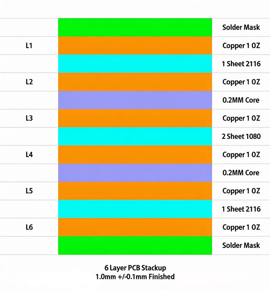
1、Structural Analysis: Why “Top-GND-Signal-Power-Signal-Bottom”?
This stackup adheres to three core principles of multi-layer PCB design: signal layers adjacent to reference planes, power-ground plane coupling, and a symmetrical structure to prevent warpage.
| Layer | Definition | Core Function | Key Design Parameters |
| L1 (Top) | Signal Layer | Placement of critical high-speed components, connectors, and top-side routing. | Impedance control ±10%, microstrip referencing L2. |
| L2 (GND) | Ground Plane | Provides a low-impedance return path for L1 and acts as a shielding layer. | Solid copper pour, avoid splits. Thickness: 3–5 mil. |
| L3 (Signal) | Signal Layer | Primary routing layer (stripline) for high-speed differential pairs. | Stripline structure referenced to L2/L4, excellent noise immunity. |
| L4 (Power) | Power Plane | Distributes multiple power rails; forms a coupling capacitor with L5. | Partitioned layout, spacing to ground plane ≤ 5 mil. |
| L5 (Signal) | Signal Layer | Auxiliary routing for low-speed signals or power routing carry-over. | References the L4 power plane; careful attention required for split plane transitions. |
| L6 (Bottom) | Signal Layer | Placement of through-hole components, test points, and bottom-side routing. | Microstrip or coplanar waveguide. |
Core Advantage: The L3 layer is sandwiched between L2 (GND) and L4 (Power), forming a perfect Stripline structure. This configuration minimizes signal radiation and provides exceptional noise immunity.
2、Application Scenario Analysis
High-Speed Digital Circuits (DDRx / PCIe / Gigabit Ethernet)
This is the most typical application scenario. When the signal rate exceeds 1 Gbps (e.g., DDR3/DDR4, PCIe 3.0, Gigabit Ethernet), Signal Integrity (SI) becomes the primary concern.
- Signal Isolation:L1 handles high-speed microstrip signals, while L3 handles high-speed stripline signals. The solid L2 ground plane ensures the shortest return path for L1 signals, reducing EMI.
- Impedance Control:Based on TORTAI Technologies’ empirical data, using this stackup with FR-4 (IT-180A) materials reliably achieves 50Ω single-ended and 100Ω differential impedance, with deviation well within ±10%.
- Case Study:A 5G CPE device utilized this structure. The DDR4 data lines (targeting 40Ω single-ended) were routed on the L3 layer. HyperLynx simulation verified an eye diagram opening of 0.8UI, confirming suitability for volume production.
Industrial and Automotive Multi-Power Domain Systems
For systems requiring multiple voltages (e.g., 12V, 5V, 3.3V, 1.8V) with significant current draw, the L4 power plane is critical.
- Power Integrity (PI):The adjacency of the L4 (Power) and L5 (GND) planes creates a low-impedance planar capacitor, effectively filtering power supply noise. According to a case study published by Jiepei PCB, this stackup significantly enhances Power Distribution Network (PDN) performance.
- Current Carrying Capacity:The copper weight on L4 can be selected between 1 oz and 2 oz. Combined with a proper via array, it can reliably carry high currents.
- Case Study:A Battery Management System (BMS) mainboard for a new energy vehicle adopted this structure. The L4 layer was partitioned into four power domains, with L2 serving as a solid ground plane. Measured power supply ripple was reduced from 200 mV to 50 mV, successfully passing the ISO 7637 standard.
High Anti-Interference Analog / Mixed-Signal Circuits
Although this stackup contains only a single dedicated ground layer (L2), careful placement and partitioning allow it to perform well in mixed-signal designs.
- Partitioning Strategy:Sensitive analog circuits (ADC/DAC) are placed on the edges of L1 or L6, away from digital noise sources. Digital signals are routed on L3, utilizing the shielding effect of the L2 ground plane to prevent digital noise from coupling into the analog domain.
- Supporting Data:An industrial data acquisition board using this structure separated the analog and digital regions with a 2 mm wide ground isolation moat on L2. The Signal-to-Noise Ratio (SNR) for the analog section improved from 60 dB to 80 dB.
3、Design Pitfalls and DFM Optimization
Avoid Direct “Signal-Signal” Adjacency
In this stackup, L3 and L5 are separated by L4 (Power). However, excessive splitting of the L4 plane can increase the coupling between L3 and L5.
- Recommendation:Prioritize routing high-speed signals on L3. Reserve L5 for low-speed signals or power routing. Avoid routing long, parallel, high-speed traces on both L3 and L5 simultaneously.
Power Plane Split Rules
When splitting the L4 power plane, follow the “20H Rule” (pull the power plane edge back 20 mil from the ground plane edge) to minimize edge radiation.
- Via Stitching:Place power vias as close as possible to the load. Place ground vias nearby to provide the shortest possible return current path.
TORTAI Technologies’ DFM Recommendations
Based on TORTAI Technologies’ PCBA manufacturing experience, common fabrication challenges with this stackup include:
- Layer Misregistration:Registration accuracy between the L3, L4, and L5 layers must be tightly controlled (within ±3 mil), otherwise the impedance will deviate significantly.
- “False 8-Layer” Trap:When the board thickness is ≥ 1.6 mm, ensuring the 50Ω impedance from L1 to L2 often requires a very thin dielectric between L2 and L3 (e.g., 3–5 mil). This necessitates a very thick prepreg stack between L3 and L4, which may exceed the manufacturer’s standard lamination limits (typically a maximum of 3 sheets of 7628 glass fabric). In this case, a core without copper (a “dummy” layer) must be added, effectively creating an expensive “false 8-layer” stackup with a 15% cost increase. It is recommended to control the board thickness to 1.0–1.2 mm to avoid this pitfall.
4、Comparative Analysis: Why Choose This Over Other 6-Layer Stacks?
| Dimension | Top-GND-Signal-Power-Signal-Bottom | 1+4+1 (Top-GND-4 Inner-Bottom) | Recommendation |
| Routing Density | Medium (3 signal layers) | Very High (5 signal layers) | Choose 1+4+1 for high density; Top-GND-Sig-PWR-Sig-Bottom for performance. |
| Signal Quality | Excellent (L3 is pure stripline) | Good (Inner signal layers susceptible to power plane noise) | Prefer Top-GND-Sig-PWR-Sig-Bottom for high-speed signals. |
| Power Integrity | Excellent (Dedicated L4 power plane) | Average (Power handled by routing or splits) | Prefer Top-GND-Sig-PWR-Sig-Bottom for multi-power domain designs. |
| Cost | Standard 6-layer cost | Slightly lower (if inner layers omit a dedicated power plane) | Choose 1+4+1 for cost-sensitive projects. |
5、Conclusion
The Top-GND-Signal-Power-Signal-Bottom stackup has become the “go-to solution” in high-speed digital and industrial control domains due to its excellent signal isolation and stable power delivery capabilities. In 2026’s electronic design landscape, mastering this structure is key to improving the first-pass yield (FPY) of PCBA projects.
In its practice helping customers optimize 6-layer PCBA designs, TORTAI Technologies has specialized in high-reliability PCBA / OEM / ODM / EMS services for over a decade. Operating a 4,000 m² modern facility equipped with 4 fully automated high-speed SMT lines, 2 DIP assembly lines, and ICT/FCT testing lines, TORTAI holds ISO9001:2015, ISO13485, and IATF16949 certifications. We strictly adhere to the IPC-A-610J CLASS III standard and utilize an MES traceability system.
Leveraging deep practical experience in 6-layer stackup planning (validating the Top-GND-Signal-Power-Signal-Bottom structure), impedance control (achieving ±5% accuracy), power integrity optimization (reducing ripple by over 70%), and high-density SMT placement, TORTAI Technologies assists clients with early-stage DFM/DFX reviews. We provide a full-service workflow from stackup simulation to volume production yield improvement, helping customers in industrial control, automotive, and telecommunications achieve highly reliable mass production.
FAQ (Frequently Asked Questions)
Q1: What signal rates can this stackup support?
A: This structure reliably supports data rates up to 10 Gbps (e.g., DDR4-3200, PCIe 3.0, Gigabit Ethernet). For supporting 25G/56G SerDes, it is recommended to upgrade to M6/M7 grade materials and consider an 8-layer design or optimize the stackup to “Signal-GND-Signal-Power-GND-Signal” for better shielding [10].
Q2: My board only uses a single 3.3V voltage rail. Can I use the L4 layer for signal routing?
A: Yes. If the power supply requirements are simple and the current draw is low, L4 can be repurposed as a signal layer, resulting in a “Top-GND-Signal-Signal-GND-Bottom” stackup. This provides higher routing density, but careful attention must be paid to crosstalk between the two adjacent signal layers. Maintaining a layer spacing of ≥ 4 mil is recommended [7].
Q3: How can I prevent L3 signals from crossing splits in the L4 power plane?
A: This is a key risk factor for this stackup. It is recommended to route L3 traces directly over continuous areas of the L4 plane, avoiding split regions. If crossing a split is unavoidable, a ground via must be placed near the crossing point to stitch the L2 and L5 ground planes together, providing a continuous return path for the signal [11].
Q4: Will a 1.6mm board thickness force a “False 8-Layer” stackup?
A: The probability is very high. At a 1.6 mm thickness, ensuring the 50Ω impedance from L1 to L2 often requires a very thin dielectric between L2 and L3 (e.g., 3–5 mil). This necessitates a very thick prepreg stack between L3 and L4, which may exceed the manufacturer’s standard lamination limits (typically a maximum of 3 sheets of 7628 glass fabric). In this case, a core without copper (a “dummy” layer) must be added, creating a high-cost “false 8-layer” structure [1]. It is recommended to reduce the board thickness to 1.0–1.2 mm to avoid this.
Q5: Can TORTAI Technologies provide simulation verification for this stackup?
A: Yes. TORTAI Technologies has a dedicated SI/PI simulation team. We provide complimentary stackup planning advice during the New Product Introduction (NPI) phase. Using industry-standard simulation software (e.g., HyperLynx), we verify impedance continuity, signal return paths, and power plane noise to ensure the design meets mass production requirements.