


In electronic hardware R&D, a common frustration among engineers is, “The schematic simulation was flawless, so why did the prototype fail?” The answer is often found in the overlooked application of Design for Manufacturing (DFM). According to industry data, over 40% of pilot runs fail due to neglected DFM, and the cost of fixing these issues downstream is 5 to 8 times higher than optimizing the initial design.
Drawing on over a decade of experience in PCBA contract manufacturing, TORTAI Technologies has identified the five most common and costly DFM pitfalls. Here is our guide to help engineers steer clear of them.
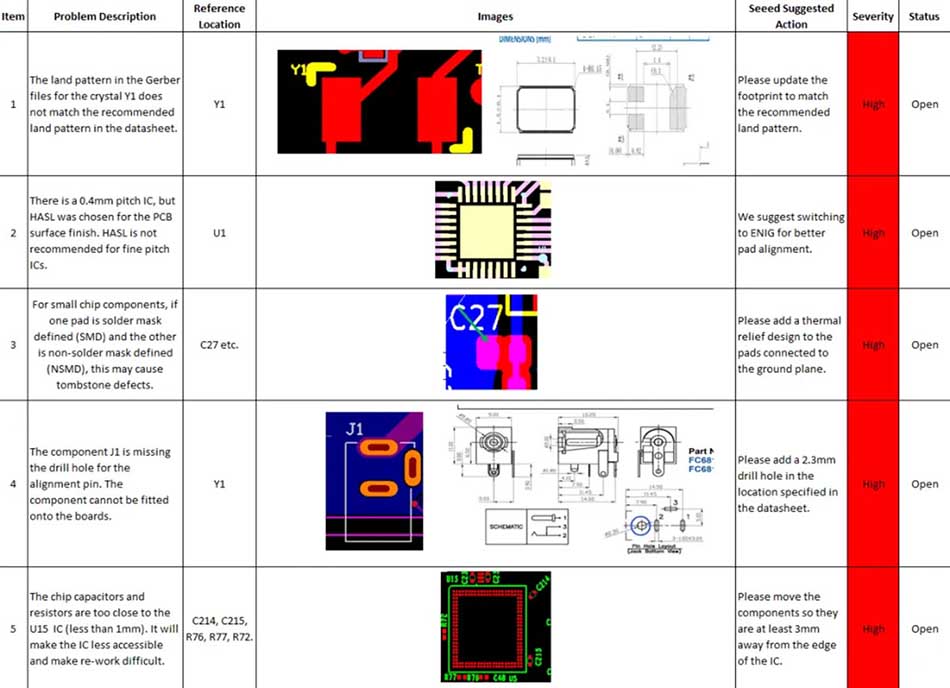
Pitfall #1: “Casual” Pad Design Leading to Tombstoning and Cold Joints
Symptoms & Risks
Many engineers simply use the default pad libraries in their EDA tools without considering the actual placement accuracy of the SMT machine or the process tolerances. For small passive components like 0402 and 0201, mismatched pad dimensions and spacing directly cause:
- Tombstoning (Manhattan Effect):Asymmetric pads or a mismatch in thermal mass cause one end of the component to lift vertically during reflow.
- Cold Joints / Solder Bridging:Overly large pads cause the solder to spread excessively, bridging to adjacent pads. Pads that are too small lead to insufficient solder volume, creating weak, unreliable joints.
Supporting Data
Industry benchmarks show that projects ignoring proper pad design experience a placement offset rate of over 20% for 0402/0201 packages and a bridging rate of up to 15% after reflow, resulting in yields below 85%. In contrast, projects strictly adhering to the IPC-7351 standard achieve offset rates under 0.5% and stable yields exceeding 99%.
The Fix
- Standardization:Strictly follow the IPC-7351 standard land pattern library. Verify pad symmetry for all two-terminal components.
- Thermal Pad Windowing:For QFN, DFN, and PowerPAD packages, the stencil aperture for the center thermal pad must be divided into a grid pattern (e.g., an 8×8 or 10×10 array with a 50–60% aperture ratio). This allows outgassing during reflow, significantly reducing voids and preventing the “Head-in-Pillow” defect.

Pitfall #2: Pushing Trace Width/Space to the Limit, Causing Etching Defects
Symptoms & Risks
To squeeze more routing into a smaller board area, engineers often push trace widths and spacing below 0.1mm (4mil). However, this typically exceeds the standard mass-production capability of most PCB manufacturers (the standard floor for reliable mass production is usually ≥ 0.1mm).
Consequences: This leads to copper slivers, open circuits, and rough impedance control during etching. The bare board yield drops drastically, leading to surcharges, schedule delays, or outright order rejection by the board house.
Supporting Data
For inner layers, the lamination process induces material shrinkage and misregistration. A trace/space of ≥ 0.18mm (7mil) is strongly recommended for inner layers of multilayer boards. For high-speed signals (e.g., USB 3.0, PCIe differential pairs), if a 0.12mm trace is required to hit a specific impedance target, you must confirm the manufacturer’s minimum etching capability and tolerance before finalizing the layout.
The Fix
- Know Your Fab’s Limits:Obtain and review your manufacturer’s official “Process Capability Specification” before starting the layout. Do not design to the absolute limit without a clear understanding of the statistical variance.
Keep a Safety Margin:
- Standard FR-4 double-sided boards: Aim for ≥ 0.15mm (6mil) trace/space.
- 4-layer and 6-layer board inner layers: Maintain ≥ 0.18mm (7mil).

Pitfall #3: Neglecting Via Design, Destroying Both Signal Integrity and Reliability
Symptoms & Risks
Improper via design is a silent killer in high-frequency and high-reliability PCBA. Common issues include:
- Excessively small hole sizes (< 0.2mm) increasing the risk of drill breakage and poor plating.
- Vias placed too close together, causing material stress and cracking (especially in thicker boards).
- Placing vias arbitrarily on SMD pads (Via-in-Pad) without proper treatment, causing solder to wick down the barrel and starving the joint.
The Stub Effect: The unused barrel of a through-hole via (the stub) acts as a transmission line stub, introducing resonance and signal degradation. A critical rule of thumb is:
Stub Length (in inches) × Resonant Frequency (GHz) ≈ 0.3
A 1.27mm (50mil) stub can cause a severe resonant dip at 6 GHz, completely corrupting a high-speed serial data stream.
Supporting Data
Each via introduces roughly 0.5 – 1.0 nH of parasitic inductance. For signals with fast edge rates (rise time ≤ 1 ns), the cumulative effect of several vias on a single net can cause the instantaneous impedance to drop from a controlled 50Ω down to 25–35Ω, leading to significant signal reflection and jitter.
The Fix
Sizing & Spacing:
- Finished hole size ≥ 0.2mm (8mil).
- Antipad (via clearance to surrounding copper) ≥ 0.2mm.
- Center-to-center via spacing ≥ 0.5mm (20mil). Keep vias at least 0.2mm from SMD pads.
Back Drilling / HDI:For any signal running at data rates > 5 Gbps (e.g., PCIe Gen 4/5, 25G+ SerDes), you must specify back drilling for through-hole vias to remove the stub, or design with HDI blind/buried vias from the start.
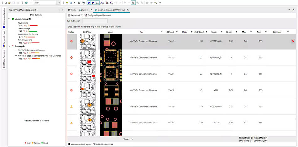
Pitfall #4: Layout Overlooking Process Keep-Outs, Destroying Board-Edge Components
Symptoms & Risks
Engineers often focus exclusively on electrical connectivity during layout, completely forgetting the physical constraints of the SMT assembly line.
- Edge Keep-Outs:The grippers and conveyor rails on a pick-and-place machine require clearance to clamp and transport the PCB. If components are placed too close to the board edge (< 3mm), they will be physically struck by the gripper, causing damage, misalignment, or tombstoning.
- Panelization & Fiducial Marks:If there are no global fiducials, or if they are obscured by solder mask or silkscreen, the machine cannot properly align the PCB.
Supporting Data
In one documented case, silkscreen text overlapping the pins of a 0.3mm pitch QFP caused the AOI system to produce a false positive rate of 12% for bridging defects, triggering unnecessary manual rework. Proper layout planning can boost test throughput yield from less than 80% to over 98%.
The Fix
- Keep-Out Zone:Reserve a keep-out zone of ≥ 3mm from the PCB edge. Components should be placed ≥ 0.5mm from the edge. For small panels, always design with tooling rails (process edges) attached via V-scoring or mouse bites.
Fiducial Marks:
- Place at least 3 global fiducials per panel in an asymmetric pattern.
- Standard fiducial size: 1.0mm solid copper circle.
- Clearance zone: 3mm radius around the fiducial must be free of copper and solder mask.
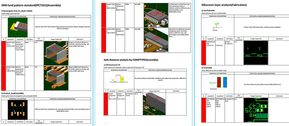
Pitfall #5: Ambiguous BOM and File Deliverables, Skyrocketing Manufacturing Communication Costs
Symptoms & Risks
This is the most common starting line error. Many engineers simply email a zipped Gerber folder without a dedicated fabrication drawing or readme file.
Consequences: This forces the factory to make assumptions about the stack-up, impedance targets, copper weights, and special process requirements (like back drilling, resin via plugging, or specific laminate materials). For example, a 12-layer AI server motherboard designed for M6/M7 ultra-low-loss laminates might be built by the factory with standard FR-4 by default, completely destroying the signal integrity for 112G SerDes lanes.
Supporting Data
A well-organized, unambiguous BOM can reduce production communication and clarification costs by over 30%. If the approved vendor list (AVL) and authorized alternate part numbers are not clearly defined, procurement lead times can easily be extended by two weeks while the buyer waits for clarification.
The Fix
Fabrication Notes:Always include a detailed PDF or text document titled “Fabrication Notes” with your Gerber package. This document must specify:
- Laminate Material (e.g., FR-4 TG170, Rogers 4350B, Megtron 7)
- Finished Board Thickness & Copper Weight
- Target Impedance Values for all controlled nets
- Required Surface Finish (ENIG, HASL LF, OSP, Immersion Silver)
- Special Processes (Back drilling, Resin plugging, Conformal coating)
Standardized BOM:The BOM must be complete and unambiguous. It must include:
- Reference Designator
- Exact Manufacturer Part Number (MPN)
- Preferred Manufacturer(s) / Brand(s)
- Package Type
- Quantity per Board
- Clearly defined column for Approved Alternates / Cross-references
Conclusion: DFM is Your Most Critical Engineering Guardian Angel
Avoiding these five pitfalls can reliably push your PCBA first-pass yield (FPY) to over 99%, dramatically shorten manufacturing lead times, and significantly reduce overall product development and rework costs.
TORTAI Technologies strongly recommends integrating a formal, standardized DFM review gate into your product development process. This allows you to catch these fundamental issues before the design is released to the board house, where they become expensive and time-consuming problems.
About TORTAI Technologies
In our practice of helping customers mitigate DFM risks, TORTAI Technologies Co., Ltd. has specialized in high-reliability PCBA / OEM / ODM / EMS for over a decade. We operate a state-of-the-art 4,000 m² facility featuring 4 fully automatic high-speed SMT lines, 2 DIP insertion lines, and dedicated ICT & FCT testing bays. We are certified to ISO 9001:2015, ISO 13485, and IATF 16949, strictly adhere to the IPC-A-610J Class III standard, and utilize a full MES traceability system.
Leveraging our deep practical experience in pad standardization, trace/space rule validation, via stub optimization (back drilling / HDI), board-edge keep-out management, and standardized BOM delivery, TORTAI Technologies assists clients in comprehensive DFM/DFX reviews early in the design cycle. We offer an end-to-end service, from “Layout Rule Checks” to “Mass Production File Validation,” helping our customers transform potential design flaws into a concrete manufacturing advantage for industrial, automotive, medical, and AI computing hardware.

Frequently Asked Questions (FAQ)
Q1: Why do pads that strictly follow IPC library standards still experience displacement during pick and place?
A: Besides the pad dimensions, you must consider the stencil thickness, the accuracy of the solder paste printer, and the repeat placement accuracy of the pick-and-place machine (typically ±0.03mm to ±0.05mm). In some cases, a slight lengthening of the pad footprint (e.g., extending a 0402 pad length from 0.6mm to 0.65mm) can be a practical way to compensate for the cumulative system tolerances.
Q2: What is the harm of “orphan copper” or “copper islands” in a PCB design?
A: When a small, isolated copper area (< 2mm²) is left electrically floating (unconnected to ground or a power net), it is prone to forming sharp slivers during etching. These slivers can break off and cause random shorts. It is critical to enable the “Copper Sliver Check” or “Unconnected Copper” DRC rule in your EDA software, setting a minimum copper area threshold (e.g., 0.5mm²).
Q3: What is the difference between NSMD and SMD pad design for BGAs?
A: NSMD (Non-Solder Mask Defined): The solder mask opening is slightly larger than the copper pad. This allows the solder to wrap around and wet the vertical sides of the copper pad, offering a stronger solder joint with a visible fillet. It is generally recommended for BGAs with a pitch of 0.5mm or greater.
SMD (Solder Mask Defined): The solder mask overlaps the edge of the copper pad, effectively defining the size of the pad. It is mechanically a bit weaker than NSMD, but can be advantageous for very fine pitches (e.g., < 0.4mm) where the mask acts as a physical dam to prevent bridging during reflow.
Q4: What are the key design rules for Test Points (Test Pads)?
A: Test points must be designed to ensure reliable contact by ICT (In-Circuit Test) probes. Key rules: diameter ≥ 0.8mm; center-to-center spacing ≥ 1.2mm (to prevent probe collisions); they must not be obstructed by components, silkscreen, or solder mask; they should be kept a safe distance from the board edge (> 2mm); ICT test coverage should target ≥ 90% of critical nodes.
Q5: Can TORTAI Technologies assist with a DFM review for my project?
A: Absolutely. TORTAI Technologies offers a free NPI (New Product Introduction) DFM pre-review service. Our engineering team will perform a comprehensive audit of your Gerber files and BOM against our actual manufacturing capabilities (including minimum line width, hole size, BGA pitch, material options, and process limits). We will provide you with a detailed Engineering Pre-Review Report within 24 hours, clearly identifying any risks and proposing solutions to ensure your design is fully optimized for high-yield mass production.